This module is marketed as super efficient (even at lower output powers) not requiring a heat sink for 100W output. Whats interesting for me is that the operating voltage is high (80V abs max) and the thermal resistance to the case isn't that high (4C/W). I'm thinking with a bit of heatsinking and a multilayer board with thermal vias for real world signal crest factors in excess of 6dB this amplifier could be bridged into 4 ohms loads and not overheat.
This is an app note where a small heatsink is applied and continuous ratings of 130W achieved and also peak power up to 220W with a heatsink:
https://www.infineon.com/dgdl/iraudamp12.pdf?fileId=5546d462533600a401535697359c2bdd
I guess what would stop this working would be if the chip started to limit output current and/or some other mechanism caused high distortion. The datasheet does have an over current protection block shown in the block diagram which is set to 16A limiting peak power to ~500W.
Seems to be a lot of advantages for the usual TI parts and I can't find any DIY discussion.
Anyway thoughts?
Hi Kipman725
I have designed a PCB for IR4302 (dual channel ... otherwise same as IR4301), but have not yet got them produced as I have other projects in the making.
I think what puts most people off is the difficulties in soldering these chips .... not really straight forward.
Secondly, it is still only 80V, so only good up to some +100W really. But at that level they are also a really good option.
I'm working on a AD1701 board as well, so thinking of making a 5x10cm board with a AD1701 and a IR4302 to form a small "plate amp" option for small 2 ways.
If you want higher power you should for sure go for a IRS2092 implementation. It's the same controlling part as in the IR430x but you have a possibility to go to max +-100Vdc .... so if we are talking 500W this is the way to go. I have worked with these chips for a long time and with only good results. You can make a better/different fb topology than what is presented in all the App notes. I use a dual bf option with both pre and post filter fb.
As for cooling of IR430x, you should cool them from the underside of the board, not on top of the chip package. You need to use 2 layer PCB and use a number of vias to connect the hot pads on the top side with the back side of the PCB. Place a small heat sink on top of that.
In my experience, the output coil will in many cases get hotter than the chip/output fets.
This is somewhat determined by the sw freq (higher is better), core size, DC voltage and wire thickness.
/Baldin
An external switch class-D would be better in many ways but it would not be as small and achieving the very high efficiency of the IR parts at low output power would be tricky. The 500W projection was based on 4ohms and running two chips per channel bridged to get double the voltage swing with the constraint of not triggering the over current protect. My interest is for my battery powered system where I'm using 3*: TPA3251-2CH-140W | 3e Audio
at the moment as a proof of concept using a buck converter from a 16S lithium ion battery (upto 67.2V). I would like to integrate everything onto a single board (DSP+AMPS) like you. With the TPA3251 ICs the board space required per IC is pretty huge and I need that additional buck converter. Getting heat out of the base of the IC is no problem I can do a much better job than the application note using a 0.8mm thick PCB and thermal vias. Beyond the 16A over current protect and the difficulty getting the heat out of a small package I can't see any issue? I guess a prototype is in order...
at the moment as a proof of concept using a buck converter from a 16S lithium ion battery (upto 67.2V). I would like to integrate everything onto a single board (DSP+AMPS) like you. With the TPA3251 ICs the board space required per IC is pretty huge and I need that additional buck converter. Getting heat out of the base of the IC is no problem I can do a much better job than the application note using a 0.8mm thick PCB and thermal vias. Beyond the 16A over current protect and the difficulty getting the heat out of a small package I can't see any issue? I guess a prototype is in order...
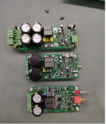
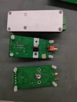
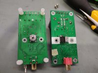
Actually, this chip is not so efficient as it mentioned in the application note. It do need the heatsink with high power output.
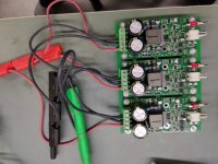
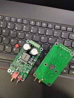
I make some boards with this chip, with dual 32V supply, it can get 120W @ 1% THD with 4 OHM load if you dissipate its heat well.(I use the SMD stud and burnt TO-220 transistor as the heatsink") )
)
I'll show some pictures as below.
I make some boards with this chip, with dual 32V supply, it can get 120W @ 1% THD with 4 OHM load if you dissipate its heat well.(I use the SMD stud and burnt TO-220 transistor as the heatsink
)I'll show some pictures as below.
Attachments
Erica.C the IC is on the top layer? if so I think significant reductions in thermal resistance from the junction can be made. Did your board do 120W continuous with the pictured heat-sink?
Here is a load of testing data on a bottom side package:
https://gansystems.com/wp-content/u...rmal-Design-Guide-Enhancement-Mode-031815.pdf
the thermal vias are the largest contribution to the thermal resistance so covering a larger area than the package and using a thinner board can make a big difference.
IR have a reputation for over-inflated ratings in their datasheets IMO, I've seen TO220 MOSFETs they rate at 100's of amps for instance, which is marketing tosh - in a foot-note somewhere they admit this is the "die limit" (probably in liquid nitrogen!)
This is a 5x6mm chip with 30 and 39 milliohm FETs, do the calculations and you'll see it needs to be mounted on 2oz IMS PCB for realistic thermal management - if you want to run at continuous high powers use discrete FETs with good heatsinking possibilities, or use an IMS breakout for this chip.
This device allows good headroom at lower powers of course.
Using aluminum PCB inserts into a normal PCB seems like a good idea for this part. This is a process I have seen used where an internal cut out is made in the FR4 board for a small alu board holding the power devce and copper tape soldered over the gap between the boards. I had a quick look at ALLPCB and 10 30*30mm ALU boards are between $8 and $17. 39m ohm doesn't seem bad to me, that's only 10W of conduction loss at 16A.
RDSon is about half the value compared to TI TPA325x. Besides this the split supply and the DIY-unfriendly case make these chips not attractive for me. I prefer a single supply full bridge as preferrable topology for battery operation and for the lack of bus pumping as well.
Just my 2c.
Just my 2c.
Erica.C the IC is on the top layer? if so I think significant reductions in thermal resistance from the junction can be made. Did your board do 120W continuous with the pictured heat-sink?
Here is a load of testing data on a bottom side package:
https://gansystems.com/wp-content/u...rmal-Design-Guide-Enhancement-Mode-031815.pdf
the thermal vias are the largest contribution to the thermal resistance so covering a larger area than the package and using a thinner board can make a big difference.
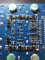
Yes, the AMP IC is on the top side, and some Vias connect with the VS pad, then the bottom side SMD stud is connect with these vias to dissipate its heat, with this stud on my board, i can get near 30W continuous power output with 4ohm load under open area. i think this is enough in reality.
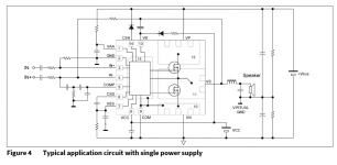
I have been working on my implementation of this chip. I was a bit perplexed at how brief the datasheet was but it turns out there are a number of helper documents:
https://www.infineon.com/dgdl/Infin...N.pdf?fileId=5546d46258fc0bc101598b13dd7d2d56
https://www.infineon.com/dgdl/Infin...N.pdf?fileId=5546d462533600a40153559b1bcc115c
https://www.infineon.com/dgdl/an-1164.pdf?fileId=5546d462533600a40153559a9bd31120
In my single supply design I have: CSH =64V, VAA = 9.6V, GND = 4.3V, VSS = 0V so that the floating analog supply is referenced to 0V and I shouldn't need coupling capacitors for the differential input to the IC. I think this is OK as per the datasheet limits? I will share a schematic of the alu daughter board when I'm done.
Yes, the AMP IC is on the top side, and some Vias connect with the VS pad, then the bottom side SMD stud is connect with these vias to dissipate its heat, with this stud on my board, i can get near 30W continuous power output with 4ohm load under open area. i think this is enough in reality.
Nice boards

I kind of like the stud idea. Have also seen this used in e.g. Powersoft LiteMod amps ... see picture ..... but these need to be solid alu or copper I think.
The upper side of a TO220 will not conduct heat very easily ....
Have been looking for these kind of studs or spacers ... what is it for a alu stud you are using? ....
if you use a heatsink directly, the side of the PCB needs to be without components and through hole components ....
Also designing pcb mounted power components one should use as much copper area as possible for heatsinking directly from the PCB itself
PS. How do you solder the IR43xx chip ... hot air?? .... have been looking to buy a cheap hot air gun on ebay ... but not sure if they are any good ....
Attachments
Last edited:
Do you know any part numbers for the solderable studs like the powersoft uses?
my construction plan was to have someone else solder the IR4301 for me but if I had to do it myself I would use a board preheater and hot air, very hard though without a stencil to apply the solder paste.
my construction plan was to have someone else solder the IR4301 for me but if I had to do it myself I would use a board preheater and hot air, very hard though without a stencil to apply the solder paste.
Last edited:
hmm I think now that the floating analog supply (VAA/VSS) must have to be centered about 1/2 the DC bus voltage otherwise there will be a DC offset present at the output due to the feedback resistor Rfb.
Using the floating supply capability is in many ways a simplification but seamed a bit power inefficient. The recommended floating supply zenner diode current is 1 - 15 mA (a bit of a big range!) and worse case 1.2W dissipation with a 80V supply. No indication of an optimal value I guess I will have to reverse engineer some dev board schematic!
Using the floating supply capability is in many ways a simplification but seamed a bit power inefficient. The recommended floating supply zenner diode current is 1 - 15 mA (a bit of a big range!) and worse case 1.2W dissipation with a 80V supply. No indication of an optimal value I guess I will have to reverse engineer some dev board schematic!
Attachments
Well the mystery deepens. The IRAUDAMP17 design runs upto 27mA of VAA/VSS current at its maximum 54 volts which is beyond the absolute maximum rating of its internal zenner diodes (20mA) and so it has external zenner diodes! so perhaps performance isn't very good at low zenner diode currents? I shall start with the minimum 1mA @ 30V supply and work up from there if I have issues.
Nice boards
I kind of like the stud idea. Have also seen this used in e.g. Powersoft LiteMod amps ... see picture ..... but these need to be solid alu or copper I think.
The upper side of a TO220 will not conduct heat very easily ....
Have been looking for these kind of studs or spacers ... what is it for a alu stud you are using? ....
if you use a heatsink directly, the side of the PCB needs to be without components and through hole components ....
Also designing pcb mounted power components one should use as much copper area as possible for heatsinking directly from the PCB itself
PS. How do you solder the IR43xx chip ... hot air?? .... have been looking to buy a cheap hot air gun on ebay ... but not sure if they are any good ....
Hi, Baldin
Happy new year
.I'm glad this design can give you some hints. And I use the hot air gun to solder this IC. It's not so difficult if you have some try.
For the stud heatsink, I use the PCB SMD NUT, it's standard part, try to google it, you'll get a lot.
BTW, my design of this IR4301 amp module is not follow the application note. It's the post-filter feedback. Indeed, the IR4301 is IRS2092 + powerstage, so you can implement it with the post filter design.
great tip I'm sure I will be able to find a lot better info now.IR4301 is IRS2092 + powerstage
Incidentally the datasheet for the IRS2092:
https://www.infineon.com/dgdl/irs2092.pdf?fileId=5546d462533600a401535675f1be2790
has 11mA of zenner diode current (which is listed as the recommend maximum for this part).
I'm going to do a non-PFFB design to start with as I want to see how much power I can get from these chips using alu core PCB and bridged and want to keep everything else as simple as possible.
- Status
- This old topic is closed. If you want to reopen this topic, contact a moderator using the "Report Post" button.
- Home
- Amplifiers
- Class D
- IR4301