In this post I’ll explain how to choose the values of various components from my versions of the circuits.
Let’s start with Denoisator + CCS, I’ll use 12Vout for my examples.
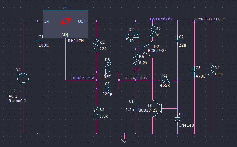
Vout is set with R2/R3 as it normally is for LM317.
R4 is just a sim load for about 100mA.
C3 should be 470uF to 1000uF to cover most Vout configurations. A minimum of 470uF makes for a reasonable Q1 base startup surge current.
C5 is 220uF for 12Vout. Try and keep a similar corner frequency for C5/R3 for different Vout. Lower Vout higher C5.
Q1 should be BC817/BC337 in -25 gain variant. Higher gain versions would make for a higher R1 value which might make it unpractical. For lowest noise use ZTX851.
Q2 can be higher gain, your choice. Just use a low noise BJT in this spot. ZTX951 doesn’t make a difference here.
D2 should be a IR LED with a Vdrop of 1-1.1V. These can be sourced from older remotes (TV/VCR etc). You could also use the IR LED from an optical isolator. If its Vdrop measures 1-1.1V on DMM then it should be ok.
Vdrop across CCS needs to be at minimum in the vicinity of 1.25V (Vout-Vadj). That’s possible with an IR LED.
R6 has to set about 1-2mA through the LED.
R5 sets the denoiser current and 50R should make for about 7.5mA. 100R for about 4mA. I’d say choose anything between these values. Should be fine.
C1 should be 3.3nF or even 4.7nF if you want to make sure.
R1 sets Vce of Q1 and we need to choose a Vce level that works with D3 startup swing limiting diode (or diode string).
Vce of Q1 varies with temperature. Simulation shows about 1.2V between 25-75 degrees C. We need to choose a Vdrop for D3 that is a bit higher than this max 1.2V variation between operating temperature extremes. Say a 1.7Vdrop red LED or 3-4x1N4148 diodes in series. Higher Vdrop means less startup swing attenuation and a longer diode string/combo (you can mix regular diodes with LEDs and Schottkys but no Zeners). So try to keep this Vdrop as small as practical.
Q1 Vce always needs to be lower than Vadj voltage such that C5 isn’t reverse biased. But we can’t go lower than Vadj – D3 Vdrop as D3 would DC-couple the denoiser. Hence why D3’s Vdrop needs to be a bit higher than Vce tempco variation between coldest day startup and hottest operating temperature.
In practice the hotter Q1 gets the lower its Vce goes. So on cold days startup it will have the highest Vce, or minimum voltage across C5. Say we set Vce such that there’s 0.3V across C5. On very cold days this might go even lower but even if it reverse biases C5 it won’t for long as it heats up due to the few mA of the denoiser circuit.
Worst case at higher operating temperatures the voltage across C5 will increase but it can’t past D3’s Vdrop so worst case scenario the denoiser gets DC-coupled to the LM317. That in turn will start lowering Vout with (even more) increasing temperature. Not ideal but lower is better than higher. But with 0.3V across C5 in the example of the simulation would go to a max of 0.3V + 1.2V max tempco swing so 1.5V, still lower than 1.7V of a red LED.
This might get confusing in LTSpice as for some reason tempco is inverted in the simulation. Vce goes higher with higher temp. In practice it went lower for me.
Here’s Vout=5V example:
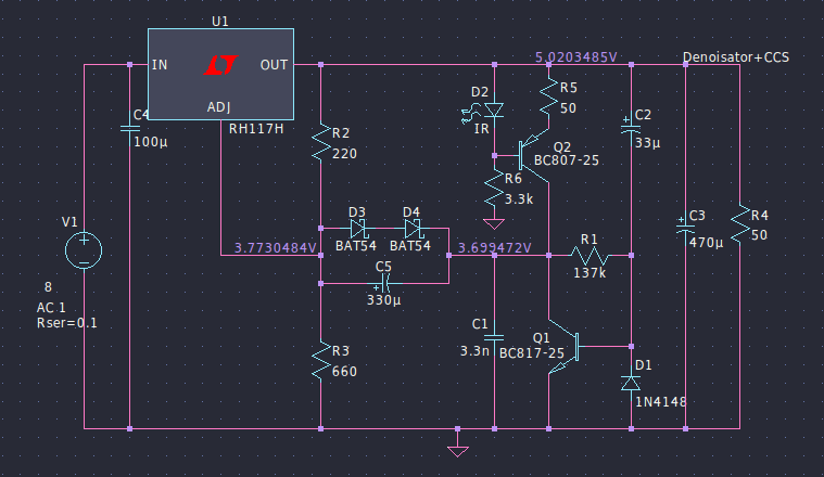
Sim shows around 0.33V tempco variation. Two Schottky diodes in series should do in this case. Vce of Q1 is set at 70mV lower than Vadj. I choose this value to be around 1/5 from diode(s) Vdrop.
So to sum it up, after you set R5/R6 and choose diode(s) Vdrop you finally get to tweak R1’s value such that you set the required Q1 Vce.
In practice it’s best to keep D3/D4 and C5 out of the circuit so that tweaking R1’s value is easier, and you don’t have any Vout swings at startup while testing. Once you set the correct voltage across C5 you can install it and diode(s) and confirm that Vce has not changed. Startup swing should now be low at startup and denoiser should stay AC-coupled after it settles.
R1’s value from the simulation should be a general starting point, it will vary from BJT to BJT.
For the DC-coupled denoiser version you set Vout with R1. There’s no startup swing or coupling cap.
For the NoNoiser same info applies:
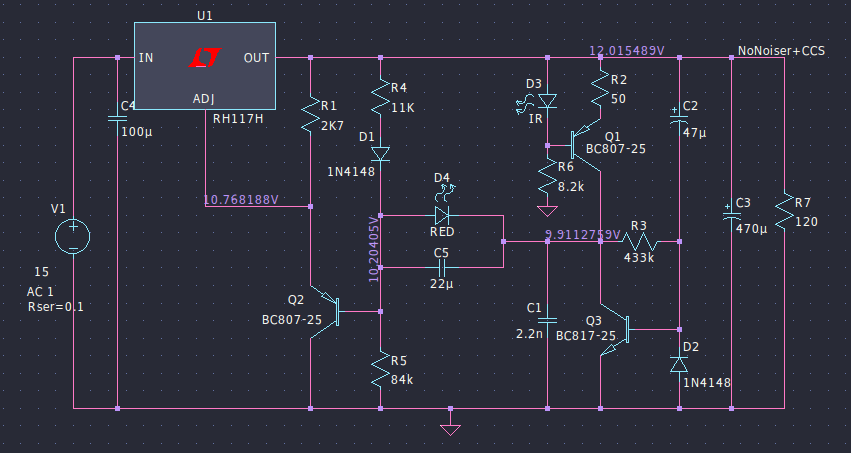
R1 should be 2.7K
Q2 use something low noise, BC807/BC327 should be fine.
R4 keep at 11K
R5 sets Vout. Vout might vary a bit vs simulation (depends on Q2 as well).
C1 should rather be 3.3nF or even 4.7nF.
In the NoNoiser case we use Q2’s base voltage instead of Vadj. Q2’s base is ~0.6V lower than Vadj. This allows for a red LED to be used in the CCS, but only for the NoNoiser as it has Q2’s Vbe in the mix.
Version with red LED in CCS:
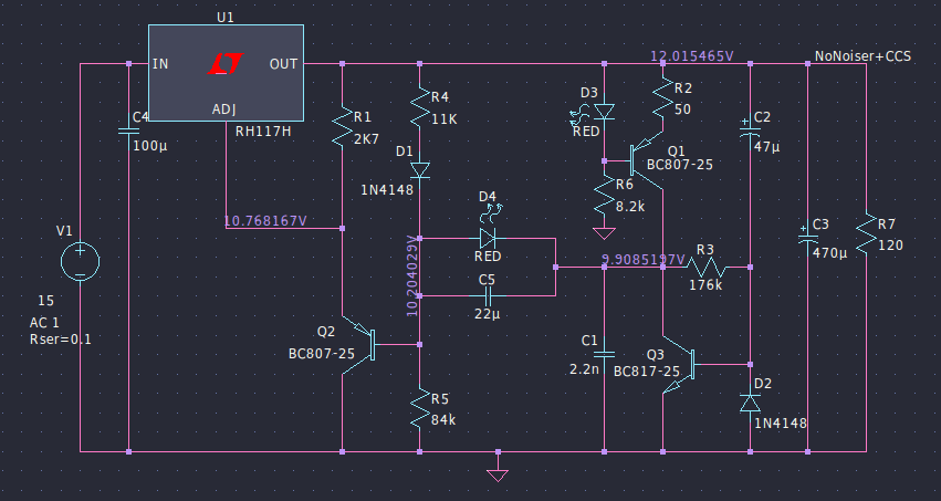
Notice the difference in R3 value for the same Q3 Vce. R3 should be the last value you set. R2/R6/D3 values affect R3’s value. Which in turn might require C2’s value to be adjusted, but that’s not critical.
The biggest downside to my versions of the denoiser is the need to manually tweak R3.
I have not tested higher Vout. Most tests were for 3.3V to around 12V. I’d say these circuits should be usable up to 24Vout. Might work for higher but I didn’t test it and there might be unforeseen surprises.
Hope this post helps with figuring out part values for your needed Vout. If something doesn’t make sense you can ask here and I’ll try to help. I also attached a LTSpice sim file with Denoisator+CCS (AC and DC coupled versions) and NoNoiser, to help with working out part values.
Now I have to review and sort out the pcb designs.
Let’s start with Denoisator + CCS, I’ll use 12Vout for my examples.
Vout is set with R2/R3 as it normally is for LM317.
R4 is just a sim load for about 100mA.
C3 should be 470uF to 1000uF to cover most Vout configurations. A minimum of 470uF makes for a reasonable Q1 base startup surge current.
C5 is 220uF for 12Vout. Try and keep a similar corner frequency for C5/R3 for different Vout. Lower Vout higher C5.
Q1 should be BC817/BC337 in -25 gain variant. Higher gain versions would make for a higher R1 value which might make it unpractical. For lowest noise use ZTX851.
Q2 can be higher gain, your choice. Just use a low noise BJT in this spot. ZTX951 doesn’t make a difference here.
D2 should be a IR LED with a Vdrop of 1-1.1V. These can be sourced from older remotes (TV/VCR etc). You could also use the IR LED from an optical isolator. If its Vdrop measures 1-1.1V on DMM then it should be ok.
Vdrop across CCS needs to be at minimum in the vicinity of 1.25V (Vout-Vadj). That’s possible with an IR LED.
R6 has to set about 1-2mA through the LED.
R5 sets the denoiser current and 50R should make for about 7.5mA. 100R for about 4mA. I’d say choose anything between these values. Should be fine.
C1 should be 3.3nF or even 4.7nF if you want to make sure.
R1 sets Vce of Q1 and we need to choose a Vce level that works with D3 startup swing limiting diode (or diode string).
Vce of Q1 varies with temperature. Simulation shows about 1.2V between 25-75 degrees C. We need to choose a Vdrop for D3 that is a bit higher than this max 1.2V variation between operating temperature extremes. Say a 1.7Vdrop red LED or 3-4x1N4148 diodes in series. Higher Vdrop means less startup swing attenuation and a longer diode string/combo (you can mix regular diodes with LEDs and Schottkys but no Zeners). So try to keep this Vdrop as small as practical.
Q1 Vce always needs to be lower than Vadj voltage such that C5 isn’t reverse biased. But we can’t go lower than Vadj – D3 Vdrop as D3 would DC-couple the denoiser. Hence why D3’s Vdrop needs to be a bit higher than Vce tempco variation between coldest day startup and hottest operating temperature.
In practice the hotter Q1 gets the lower its Vce goes. So on cold days startup it will have the highest Vce, or minimum voltage across C5. Say we set Vce such that there’s 0.3V across C5. On very cold days this might go even lower but even if it reverse biases C5 it won’t for long as it heats up due to the few mA of the denoiser circuit.
Worst case at higher operating temperatures the voltage across C5 will increase but it can’t past D3’s Vdrop so worst case scenario the denoiser gets DC-coupled to the LM317. That in turn will start lowering Vout with (even more) increasing temperature. Not ideal but lower is better than higher. But with 0.3V across C5 in the example of the simulation would go to a max of 0.3V + 1.2V max tempco swing so 1.5V, still lower than 1.7V of a red LED.
This might get confusing in LTSpice as for some reason tempco is inverted in the simulation. Vce goes higher with higher temp. In practice it went lower for me.
Here’s Vout=5V example:
Sim shows around 0.33V tempco variation. Two Schottky diodes in series should do in this case. Vce of Q1 is set at 70mV lower than Vadj. I choose this value to be around 1/5 from diode(s) Vdrop.
So to sum it up, after you set R5/R6 and choose diode(s) Vdrop you finally get to tweak R1’s value such that you set the required Q1 Vce.
In practice it’s best to keep D3/D4 and C5 out of the circuit so that tweaking R1’s value is easier, and you don’t have any Vout swings at startup while testing. Once you set the correct voltage across C5 you can install it and diode(s) and confirm that Vce has not changed. Startup swing should now be low at startup and denoiser should stay AC-coupled after it settles.
R1’s value from the simulation should be a general starting point, it will vary from BJT to BJT.
For the DC-coupled denoiser version you set Vout with R1. There’s no startup swing or coupling cap.
For the NoNoiser same info applies:
R1 should be 2.7K
Q2 use something low noise, BC807/BC327 should be fine.
R4 keep at 11K
R5 sets Vout. Vout might vary a bit vs simulation (depends on Q2 as well).
C1 should rather be 3.3nF or even 4.7nF.
In the NoNoiser case we use Q2’s base voltage instead of Vadj. Q2’s base is ~0.6V lower than Vadj. This allows for a red LED to be used in the CCS, but only for the NoNoiser as it has Q2’s Vbe in the mix.
Version with red LED in CCS:
Notice the difference in R3 value for the same Q3 Vce. R3 should be the last value you set. R2/R6/D3 values affect R3’s value. Which in turn might require C2’s value to be adjusted, but that’s not critical.
The biggest downside to my versions of the denoiser is the need to manually tweak R3.
I have not tested higher Vout. Most tests were for 3.3V to around 12V. I’d say these circuits should be usable up to 24Vout. Might work for higher but I didn’t test it and there might be unforeseen surprises.
Hope this post helps with figuring out part values for your needed Vout. If something doesn’t make sense you can ask here and I’ll try to help. I also attached a LTSpice sim file with Denoisator+CCS (AC and DC coupled versions) and NoNoiser, to help with working out part values.
Now I have to review and sort out the pcb designs.
Attachments
Looking at the index and the boards you linked I don't think I can add anything else.
I've gone through quite a few iterations along the way but the one you linked as recommended by me are ok.
The others are either not fully tested, either don't contain the CCS, or don't have an optimized layout.
I've gone through quite a few iterations along the way but the one you linked as recommended by me are ok.
The others are either not fully tested, either don't contain the CCS, or don't have an optimized layout.
In this post I’ll explain how to choose the values of various components from my versions of the circuits.
Let’s start with Denoisator + CCS, I’ll use 12Vout for my examples.
View attachment 1104835
Vout is set with R2/R3 as it normally is for LM317.
R4 is just a sim load for about 100mA.
C3 should be 470uF to 1000uF to cover most Vout configurations. A minimum of 470uF makes for a reasonable Q1 base startup surge current.
C5 is 220uF for 12Vout. Try and keep a similar corner frequency for C5/R3 for different Vout. Lower Vout higher C5.
Q1 should be BC817/BC337 in -25 gain variant. Higher gain versions would make for a higher R1 value which might make it unpractical. For lowest noise use ZTX851.
Q2 can be higher gain, your choice. Just use a low noise BJT in this spot. ZTX951 doesn’t make a difference here.
D2 should be a IR LED with a Vdrop of 1-1.1V. These can be sourced from older remotes (TV/VCR etc). You could also use the IR LED from an optical isolator. If its Vdrop measures 1-1.1V on DMM then it should be ok.
Vdrop across CCS needs to be at minimum in the vicinity of 1.25V (Vout-Vadj). That’s possible with an IR LED.
R6 has to set about 1-2mA through the LED.
R5 sets the denoiser current and 50R should make for about 7.5mA. 100R for about 4mA. I’d say choose anything between these values. Should be fine.
C1 should be 3.3nF or even 4.7nF if you want to make sure.
R1 sets Vce of Q1 and we need to choose a Vce level that works with D3 startup swing limiting diode (or diode string).
Vce of Q1 varies with temperature. Simulation shows about 1.2V between 25-75 degrees C. We need to choose a Vdrop for D3 that is a bit higher than this max 1.2V variation between operating temperature extremes. Say a 1.7Vdrop red LED or 3-4x1N4148 diodes in series. Higher Vdrop means less startup swing attenuation and a longer diode string/combo (you can mix regular diodes with LEDs and Schottkys but no Zeners). So try to keep this Vdrop as small as practical.
Q1 Vce always needs to be lower than Vadj voltage such that C5 isn’t reverse biased. But we can’t go lower than Vadj – D3 Vdrop as D3 would DC-couple the denoiser. Hence why D3’s Vdrop needs to be a bit higher than Vce tempco variation between coldest day startup and hottest operating temperature.
In practice the hotter Q1 gets the lower its Vce goes. So on cold days startup it will have the highest Vce, or minimum voltage across C5. Say we set Vce such that there’s 0.3V across C5. On very cold days this might go even lower but even if it reverse biases C5 it won’t for long as it heats up due to the few mA of the denoiser circuit.
Worst case at higher operating temperatures the voltage across C5 will increase but it can’t past D3’s Vdrop so worst case scenario the denoiser gets DC-coupled to the LM317. That in turn will start lowering Vout with (even more) increasing temperature. Not ideal but lower is better than higher. But with 0.3V across C5 in the example of the simulation would go to a max of 0.3V + 1.2V max tempco swing so 1.5V, still lower than 1.7V of a red LED.
This might get confusing in LTSpice as for some reason tempco is inverted in the simulation. Vce goes higher with higher temp. In practice it went lower for me.
Here’s Vout=5V example:
View attachment 1104836
Sim shows around 0.33V tempco variation. Two Schottky diodes in series should do in this case. Vce of Q1 is set at 70mV lower than Vadj. I choose this value to be around 1/5 from diode(s) Vdrop.
So to sum it up, after you set R5/R6 and choose diode(s) Vdrop you finally get to tweak R1’s value such that you set the required Q1 Vce.
In practice it’s best to keep D3/D4 and C5 out of the circuit so that tweaking R1’s value is easier, and you don’t have any Vout swings at startup while testing. Once you set the correct voltage across C5 you can install it and diode(s) and confirm that Vce has not changed. Startup swing should now be low at startup and denoiser should stay AC-coupled after it settles.
R1’s value from the simulation should be a general starting point, it will vary from BJT to BJT.
For the DC-coupled denoiser version you set Vout with R1. There’s no startup swing or coupling cap.
For the NoNoiser same info applies:
View attachment 1104837
R1 should be 2.7K
Q2 use something low noise, BC807/BC327 should be fine.
R4 keep at 11K
R5 sets Vout. Vout might vary a bit vs simulation (depends on Q2 as well).
C1 should rather be 3.3nF or even 4.7nF.
In the NoNoiser case we use Q2’s base voltage instead of Vadj. Q2’s base is ~0.6V lower than Vadj. This allows for a red LED to be used in the CCS, but only for the NoNoiser as it has Q2’s Vbe in the mix.
Version with red LED in CCS:
View attachment 1104838
Notice the difference in R3 value for the same Q3 Vce. R3 should be the last value you set. R2/R6/D3 values affect R3’s value. Which in turn might require C2’s value to be adjusted, but that’s not critical.
The biggest downside to my versions of the denoiser is the need to manually tweak R3.
I have not tested higher Vout. Most tests were for 3.3V to around 12V. I’d say these circuits should be usable up to 24Vout. Might work for higher but I didn’t test it and there might be unforeseen surprises.
Hope this post helps with figuring out part values for your needed Vout. If something doesn’t make sense you can ask here and I’ll try to help. I also attached a LTSpice sim file with Denoisator+CCS (AC and DC coupled versions) and NoNoiser, to help with working out part values.
Now I have to review and sort out the pcb designs.
@Trileru also told me that C3 needs to have an ESR between 0.2 and 0.5
Does this "add-on" circuit work O.K. ?I also made two designs for adapters to existing circuits. They are compatible with De/DieNoiser variants. There's smd jumpers for all options, and smd passives are 0805.
These boards would theoretically work for 78xx regs as well, just that you need to disconnect the ground leg of the reg from the existing pcb and connect that to the adapter on the "adj" connection. I'm not sure how well it works. The resistor to ground in parallel with the cap are for 78xx regs, you don't populate that for lm317.
The tht version you could diy at home. The smd version is more for pcb house production, it would be pretty hard to diy.
tht version is around 23mm X 23 mm and smd version is around 19mm x 14mm.
Pay attention to the polarity of the 220uF cap. I've seen it wrongly added to a few schematics floating around this thread. Many issues people had might be to this as well.
I've changed the bjt to92 footprint. This allows if careful to solder the smd version of BC337/BC327 (BC817/BC807) on the same pads. Maybe someone wants to diy the board and has the smd bjt at hand.


No I don't recommend that one. I'm not sure if there's any THT add-on board designs linked in Elvee's first post.
Do you care about it being THT?
Do you care about it being THT?
Trileru - Yes - want to stick with THT. Do not need the latest-greatest. Just want something to "upgrade" some existing pieces of gear with an Add-On board, something with the least amount of overshoot - most of the units are +/- 16V and some of the onboard amps have 18V limits. I have plenty of ZTX851 and 951 - so if you could link me to something using those- great.
Then maybe something like this?
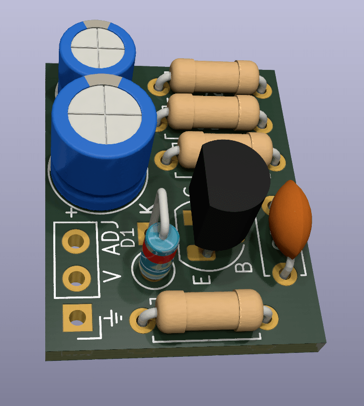
It's the original Denoisator:
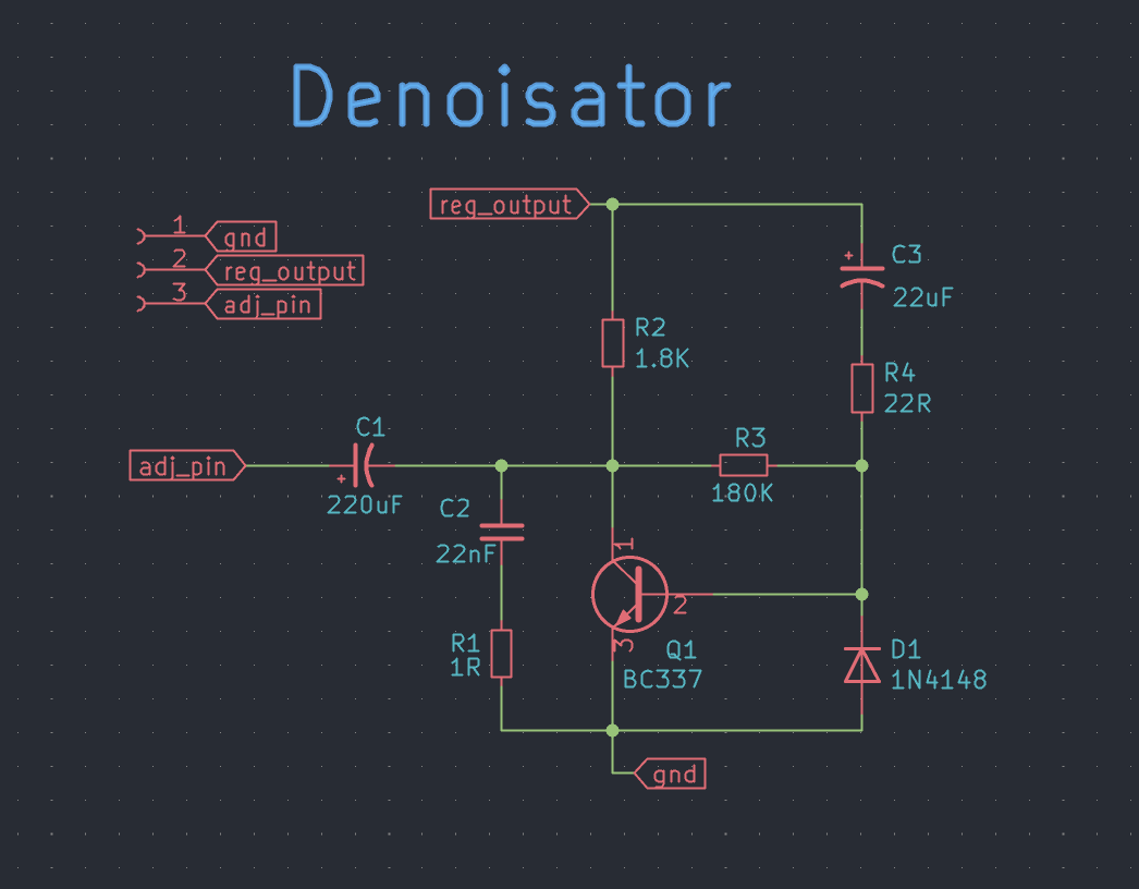
All THT. I marked BCE of Q1 on the PCB so you could add a ZTX BJT as well. Maybe Elvee can help you with part values for you needed Vout.
The larger cap is 6.3mm diameter.
The archive contains the Kicad project files as well as gerber.zip file for fab house. And the DIY PDF file.
It's the original Denoisator:
All THT. I marked BCE of Q1 on the PCB so you could add a ZTX BJT as well. Maybe Elvee can help you with part values for you needed Vout.
The larger cap is 6.3mm diameter.
The archive contains the Kicad project files as well as gerber.zip file for fab house. And the DIY PDF file.
Attachments
Trileru - this looks great. So for about $10 worth of parts and an hour or two of time - one can upgrade an audio device using 317/337 regs.
Since this is the basic Denoisator and not the Sziklai Dienoiser, isn't the voltage set with the existing on board resistors?
Since this is the basic Denoisator and not the Sziklai Dienoiser, isn't the voltage set with the existing on board resistors?
Yes but there's R2/R3 which need to be adjusted for your Vout to set the denoiser current and Vce.
With LM337 for R1 try 1R-3.9R.
For the Sziklai Dienoiser you set Vout the same, with the original resistors, but needs more compensation and I prefer to use the extra BJT for the CCS. Also for some reason output RLC network (capacitor) should have a bit of inductance for stability. That doesn't seem to be the case for the CCS Denoisator which uses a higher Vce for Q1 (~Vadj).
Hi Trileru,
do you have designed a PCB for nonoiser with BC327/337 in post #2546. thank you! Maxpou
do you have designed a PCB for nonoiser with BC327/337 in post #2546. thank you! Maxpou
Trileru - is there a formula for figuring out R2/R3 for the Denoisator add-on you sent above (#2570) ?Yes but there's R2/R3 which need to be adjusted for your Vout to set the denoiser current and Vce.
With LM337 for R1 try 1R-3.9R.
For the Sziklai Dienoiser you set Vout the same, with the original resistors, but needs more compensation and I prefer to use the extra BJT for the CCS. Also for some reason output RLC network (capacitor) should have a bit of inductance for stability. That doesn't seem to be the case for the CCS Denoisator which uses a higher Vce for Q1 (~Vadj).
I need for 16V and 28V - both run around 200ma
Elvee first showed the circuit with 1.8K/180K for about 15Vout. That means about 6mA through the denoiser and Vce of around 4V.
For your 28Vout R2 of about 3.9K keeps the same current through the denoiser and R3 of 390K makes for a Vce of around 7V. Not sure if Elvee would recommend these values. In my initial tests I tried to keep 1:100 between R2 and R3.
For your 28Vout R2 of about 3.9K keeps the same current through the denoiser and R3 of 390K makes for a Vce of around 7V. Not sure if Elvee would recommend these values. In my initial tests I tried to keep 1:100 between R2 and R3.
I honestly believe that while @Elvee being a wise man agreed for his topic to be blatantly hacked by two other users as gray haired wise men never get agressive or dismissive to youngsters, this topic should be split in three cause it's damn hard to follow this interleaved discussion . Personally I don't trust useless complications in anything and I have proof that one more transistor can spill the cofee over the table in many situations .It was already difficult for me to see the usefulness of making LM317 better while avoiding instability by adding just 1 transistor.If you get to add 5 (FIVE!!!) transistors 3 capacitors , 6 resistors and a potentiometer to an IC, then what's the value left in that IC?
An IC regulator may have 50 transiators yet it doesn't necessarily make it more capable than a 5 discrete transistor regulator.Those 50 transistors are there to make a tiny 3 pin regulator cope wirh its own size limitations .
With 5 transistors alone you can get one of the finest regulators you could possibly use in audio and no other IC is needed.
- Home
- Amplifiers
- Power Supplies
- D-Noizator: a magic active noise canceller to retrofit & upgrade any 317-based VReg