Hi,
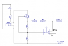
For those who are suffering with matching smd jfets I am making a small pcb. Attached schematic. Can use with SOT23 JFETS and through hole JFETS of small packages. Both N and P channel fets can be matched with changing polarity of battery connection. Also can be used with SOT23 packages with D ,S reversed.
Vp
Id for given application and Idss can be matched with minimal alteration(wire instead of resistor) .
Please see attached schematic. Point out any mistakes and improvements.
I will order PCBC in a week and anyone interested can send them for shipping and 1 $ per board.
If there is enough people may be a kit with socket pins for jumpers and testpont for multimeter etc
Ref
Transistor matching
Attachments

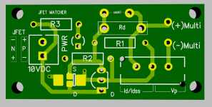
Which resistors are which?
Label the schematic and then use those labels on the top screen print.
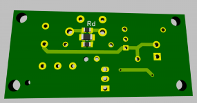
Where is Rd?
Where is JR & JR'?
What is the pin pitch of the Idss/Vp options?
Could a 0.1" shorting plug fit over the pins to be shorted?
Label the schematic and then use those labels on the top screen print.
Where is Rd?
Where is JR & JR'?
What is the pin pitch of the Idss/Vp options?
Could a 0.1" shorting plug fit over the pins to be shorted?
Last edited:
I will write up a manual for what to do with this jig but pretty much self explanatory if you are Savvy enough to match them for a purpose !
I will write up a manual for what to do with this jig but pretty much self explanatory if you are Savvy enough to match them for a purpose !
Oh, so it is a ..... PUZZLE!!!! ......

Cool, breaks down the Tech article monotony for a change.

Only you posted it on the wrong section .... it should be in http://www.diyaudio.com/forums/the-lounge/ instead.
Just one nagging question: what is the prize if I solve it?
Can I ask, say, for a little

kinku:
I agree that it would be helpful if you provided some better details, but I assume that you will do so in the manual.
I presume that a standard 9v battery can be used?
Regards,
Scott
I agree that it would be helpful if you provided some better details, but I assume that you will do so in the manual.
I presume that a standard 9v battery can be used?
Regards,
Scott
@kinku
If not to late, why not using retaining spring for SOT23 JFET?
http://www.fischerelektronik.de/web_fischer/en_GB/heatsinks/A06/Retaining%20springs%20for%20transistors/PR/THFK220_/$productCard/dimensionParameters/index.xhtml
2 cents.
JP
If not to late, why not using retaining spring for SOT23 JFET?
http://www.fischerelektronik.de/web_fischer/en_GB/heatsinks/A06/Retaining%20springs%20for%20transistors/PR/THFK220_/$productCard/dimensionParameters/index.xhtml
2 cents.
JP
You need to be able to quickly place BF862 and press in place to test then remove and do over again if you want to test circa 100 of them. I use rubber eraser on pencil to push in place manually while waiting for DVM reading to stabilize.
Cool, I want one, please! I've got this tube full of BF862 sitting around for way too long now...
Cool, I want one, please! I've got this tube full of BF862 sitting around for way too long now...
http://www.diyaudio.com/forums/swap-meet/316027-jfet-matching-jig-5.html#post5274642
JSP64, great idea ! But won't that spring shot out pads for Drain and source when JFEt is not in place ?
I am using a good old plastic cloth hanging clip ( location for JFEt on board is ideal for that.)
There is nothing complex in it. IDss is current through drain or source when source and gate are at ground potential and ID is when you add desired resistor between ground and source . I am just applying it in circuit. It is a pain to do this with SOt23 without a dedicated board.
Which resistors are which?
Label the schematic and then use those labels on the top screen print.
Where is Rd?
Where is JR & JR'?
What is the pin pitch of the Idss/Vp options?
Could a 0.1" shorting plug fit over the pins to be shorted?
Idss Vp is a slide switch,
Shorting plugs have a pin diameter of 1mm and most resistors (TH) 0.6. It is hard to find a receptacle that accept that extremes of pins. If you can suggest one happy to change it. But I will adjust the jumper pin spacing for your suggestion .
0552-1-15-01-11-27-10-0 for through hole JFET Mill-Max: 0552 - Receptacle With No Tail
0336-0-15-01-34-01-04-0 for shorting Mill-Max: 0336 - Receptacle With A Standard Tail
0338-0-15-01-15-27-10-0 for resistor pin https://www.mill-max.com/products/rec/0338
Fancy Jumper
https://www.harwin.com/products/D3087-99/
JP don't use that switch, if you want to mount it on board. pin pitch is 4 mm
by positioning two receptacles close by we can increase pin size range from 0.54 mm to 1.17mms
Last edited:
For SMD yes as the middle pin is always gate, and for most TO packages too. I don't think they make any SMD JFEt with gate at one end.
This is board is mainly for SMD though I left through hole just as an option. I would not make a PCB for through hole alone as good old direct wiring or bread board is more versatile.
But let me see!!!!!
This is board is mainly for SMD though I left through hole just as an option. I would not make a PCB for through hole alone as good old direct wiring or bread board is more versatile.
But let me see!!!!!
Last edited:
- Status
- Not open for further replies.
- Home
- Amplifiers
- Pass Labs
- SMD jfet test jig