") . All I am saying is that if you move it an inch higher, the temperature difference will probably be less than 1 degree Celsius.
. All I am saying is that if you move it an inch higher, the temperature difference will probably be less than 1 degree Celsius. Looking at my left and right channels, from the front without the front panel in place, one is a few mm higher than the other. Further inspection reveals that the heat sinks are asymmetrical top to bottom.....you might check this out and gain a bit of height by reversing the heat sinks. for me, I'm going to leave well enough alone.
Looking at my left and right channels, from the front without the front panel in place, one is a few mm higher than the other. Further inspection reveals that the heat sinks are asymmetrical top to bottom.....you might check this out and gain a bit of height by reversing the heat sinks. for me, I'm going to leave well enough alone.
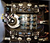
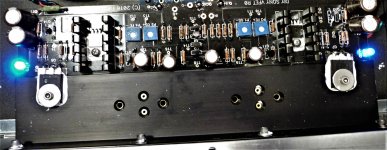
My heatsinks are not the store pre-drilled sinks you can get with the 5U/400 and 4U/300 Deluxe cases. I some odd way one cannot order pre-drilled UMS heatsinks that fits the 4U/400 case. So I can drill my own sinks whenever I am happy with my layout.
Finished my build today but have a strange problem with one (R) channel. I installed the VFETS and started out with about 30 mV across R32 before I started adjusting bias using a 1 amp fuse on the PSU and hooking up only one side at a time as Nelson suggested in his instructions. I biased up both channels to 100 mV and ~ 3 mV offset (after they had heated up for ~ 1 hr with lid on for each channel). They both biased up pretty easily and both the heat sinks got only moderately warm. I then hooked it up to some relatively cheap speakers for a test drive. No hum, no noise, silent but the right channel volume fades out and goes silent after ~ 2 seconds, the left channel is fine and sounds great. If I disconnect the source from the right channel and connect it again it plays and fades out in ~ 2 sec. There is no noise from the right channel. During the built both boards passed the resistor test (part 1) and the voltage tests (part 2) in Nelson's instructions. The parts were from the DIY Audio supplemental kit. Does anyone have any thoughts or ideas on where I should start looking ?
Attachments
Finished my build today but have a strange problem with one (R) channel. I installed the VFETS and started out with about 30 mV across R32 before I started adjusting bias using a 1 amp fuse on the PSU and hooking up only one side at a time as Nelson suggested in his instructions. I biased up both channels to 100 mV and ~ 3 mV offset (after they had heated up for ~ 1 hr with lid on for each channel). They both biased up pretty easily and both the heat sinks got only moderately warm. I then hooked it up to some relatively cheap speakers for a test drive. No hum, no noise, silent but the right channel volume fades out and goes silent after ~ 2 seconds, the left channel is fine and sounds great. If I disconnect the source from the right channel and connect it again it plays and fades out in ~ 2 sec. There is no noise from the right channel. During the built both boards passed the resistor test (part 1) and the voltage tests (part 2) in Nelson's instructions. The parts were from the DIY Audio supplemental kit. Does anyone have any thoughts or ideas on where I should start looking ?
It may be unrelated, but I think these rectifier diodes need some heatsinkig, mine are getting pretty hot...
Finished my build today but have a strange problem with one (R) channel. I installed the VFETS and started out with about 30 mV across R32 before I started adjusting bias using a 1 amp fuse on the PSU and hooking up only one side at a time as Nelson suggested in his instructions. I biased up both channels to 100 mV and ~ 3 mV offset (after they had heated up for ~ 1 hr with lid on for each channel). They both biased up pretty easily and both the heat sinks got only moderately warm. I then hooked it up to some relatively cheap speakers for a test drive. No hum, no noise, silent but the right channel volume fades out and goes silent after ~ 2 seconds, the left channel is fine and sounds great. If I disconnect the source from the right channel and connect it again it plays and fades out in ~ 2 sec. There is no noise from the right channel. During the built both boards passed the resistor test (part 1) and the voltage tests (part 2) in Nelson's instructions. The parts were from the DIY Audio supplemental kit. Does anyone have any thoughts or ideas on where I should start looking ?
What is the voltage at T18?
It should be ~0V +-200mV when all warmed up.
Today I let the amp warm up for ~ 30 -40 minutes and took some voltage readings to compare the working channel to the non-working one (right channel). Nothing really stands out as being different between the two. I have attached a copy of the readings. I also tested the continuity of the input cables from the jacks back to the board, no surprises there either. I am wondering if the input JFEts (2SJ74/2SJ170) are the problem. Is there anyway I can check them mounted in the board ?
Thanks
Paul
Thanks
Paul
Attachments
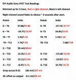
Today I let the amp warm up for ~ 30 -40 minutes and took some voltage readings to compare the working channel to the non-working one (right channel). Nothing really stands out as being different between the two. I have attached a copy of the readings. I also tested the continuity of the input cables from the jacks back to the board, no surprises there either. I am wondering if the input JFEts (2SJ74/2SJ170) are the problem. Is there anyway I can check them mounted in the board ?
Thanks
Paul
Check R4?
Check R4?
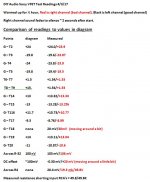
I checked R4 as well as the channel voltages against the circuit diagram. R4 is the correct value at 332R, and the measures voltages across is was 19.3 mV for the right(bad) channel and 20.4 mV for the left (good) channel. I've attached my measurements, both channels agree within reason with the guidance in Nelson's diagram. I looked over the top of the problem board with a magnifying glass, but saw nothing unusual. My next step will be to pull the board keeping it mounted from the amp case and do a thorough inspection of the bottom of the board, and reflow all of the joints and give it another try before I start pulling out parts. Does anyone have any other ideas ?
Attachments
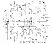
T2 to T3 is an issue. The TL reg is ok but T3 should be less the Vgs drop of Q7.
BDP
I afraid I screwed up when I typed up my readings, G-T3 was 19.43 v for right channel, 19.6 for left. Looks like also made a few other typing mistakes in my haste transferring my chicken scratch readings to a word document list. I must be typing challenged. Sorry about that.
Last edited:
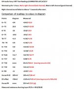
Ok, it looks like it is the front end. I played music through it and took voltage measurements at the RCA jacks and at G-T18 on both channels I got ~100mVac at the input jacks on both channels, on the good channel G-T18 was about 400 mVac and jumping around. On the bad channel I got 0 mVac. It looks like I need to pull the JFETS. Thanks
- Home
- Amplifiers
- Pass Labs
- Sony vFET Illustrated build guide