Hi,
Does anyone have information on the following transformers?
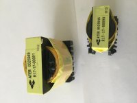
They are both out of a blown Mackie SRM1801 smps. ATAR 25949 andATAR 0025946.
Any information regarding secondary output voltages would be appreciated. Availability and/or a supplier or suitable alternative would also be appreciated.
Pics are attached.
Thank you.
Does anyone have information on the following transformers?
They are both out of a blown Mackie SRM1801 smps. ATAR 25949 andATAR 0025946.
Any information regarding secondary output voltages would be appreciated. Availability and/or a supplier or suitable alternative would also be appreciated.
Pics are attached.
Thank you.
Attachments
If they came from an SMPS, you pretty much need to find the exact thing. They are not working at mains frequencies, and won't have standard 240 to 12v ratios or such. Yours may be faulty, but in my experience, those small transformers very rarely fail. What have you determined is wrong with them? They will have naturally low resistances in the windings
I don't know which is which here, but typically one or both may provide power supply voltages, but they won't be driven by sine waves nor from mains levels. In many SMPS though the transformer may be a driver, a switching circuit pulses the transformer which in turn drives the gates of MOSFETs or other switching transistors.
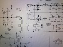
Get the schematics from Mackie. I just checked their web site, the SRM1801 is available for download. T2 is a driver type. T1 is the output. But I find way more common in SMPS are shorted rectifiers on the secondary side. And of course shorted driver switching transistors. Sometimes failed controller ICs. At the mains input stage, thoe thermistors ccan open.
If you are not familiar with SMPS service, STOP, read up on it. They can be very dangerous. They rectify and filter the mains directly. And on the primary side, all those circuits have a "ground" or common that is NOT EARTH. Note the ground symbols for that section all have the little sine wave inside. Those sit at about -170vDC with respect to earth. Connect a scope grund there and you will blow somethin gup.
I don't know which is which here, but typically one or both may provide power supply voltages, but they won't be driven by sine waves nor from mains levels. In many SMPS though the transformer may be a driver, a switching circuit pulses the transformer which in turn drives the gates of MOSFETs or other switching transistors.
Get the schematics from Mackie. I just checked their web site, the SRM1801 is available for download. T2 is a driver type. T1 is the output. But I find way more common in SMPS are shorted rectifiers on the secondary side. And of course shorted driver switching transistors. Sometimes failed controller ICs. At the mains input stage, thoe thermistors ccan open.
If you are not familiar with SMPS service, STOP, read up on it. They can be very dangerous. They rectify and filter the mains directly. And on the primary side, all those circuits have a "ground" or common that is NOT EARTH. Note the ground symbols for that section all have the little sine wave inside. Those sit at about -170vDC with respect to earth. Connect a scope grund there and you will blow somethin gup.

Thank you for the very informative response Enzo.
I am aware of the dangers of SMPSs, thank you and I will take heed of your warnings.
The 'blown' sub was given to me by are friend who hoped to repair it for himself, but could not find time to do so.
At power on, only the OL (red led), was turning on and remaining on.
On inspection of the pcb, diodes, resistors, transistors and MOSFETS between both T2 secondaries were blown, with both MOSFET showing signs of 'catastrophic failure' ie bits blow off the heat sink!!
(All of these smd components including MOSFETS were replaced).
As a result of this effort, the Power light (green LED) now turns on, although the OL red light remains on.
I have discovered the complexities of identifying the 'ground' for taking dvm readings, and my scopes are safely packed away! Thank you.
As i progress with the trouble shooting process, I am referring to SRM1801 schematics and data sheets and learning as much as I can, but of course will never be an expert or too confident. Which brings me to diyAudio, hoping to get directions on how to proceed safely.
Is it normal for these transformers to measure OL across the poles? If, as you say, the transformers rarely fail, hopefully they are still ok, I can shift my focus elsewhere.
Thanks MikePP, and egellings any input is appreciated.
Thanks again Enzo, for the effort and time taken to compose your clearly worded response any further advice will be valued.
Take care and stay safe.
Attachments
Is it normal for these transformers to measure OL across the poles?
Specifically , which poles ? (primary ? secondary ? which precise pins?)
PS: Often times the connection between the two primaries (refering to T1) is done on board , so for example if you pull T1 off the board and measure across (1,2) and (5,6) you will see O/C
PPS: Often times there are also dummy pins added for physical security
Sorry about the ambiguous nature of my question.
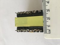
On the ATER 0025949 (see attached pic)
With the tx oriented as per attached pic:
On the bottom row of pins from left to right I get continuity on
pins 1 and 3, pins 1 and 5,
pins 2 and 4, pins 2 and 6,
pins 3 and 5,
pins 5 and 7
On the upper row of pins, from left to right I get connectivity between
Pins 1 and 3, pins 1 and 5.
Pins 2 and 4, pins 4 and 6
Pin 3 and 5
Hope this is helpful, I am unable to source a data sheet to be more specific.
If the above test proves helpful, I will repeat on the AT 0025946
Thank you MikePP
Attachments
Last edited:
Sorry about the ambiguous nature of my question.
On the ATER 0025949 (see attached pic)
With the tx oriented as per attached pic:
On the bottom row of pins from left to right I get continuity on
pins 1 and 3, pins 1 and 5,
pins 2 and 4, pins 2 and 6,
pins 3 and 5,
pins 5 and 7
On the upper row of pins, from left to right I get connectivity between
Pins 1 and 3, pins 1 and 5.
Pins 2 and 4, pins 4 and 6
Pin 3 and 5
Hope this is helpful, I am unable to source a data sheet to be more specific.
If the above test proves helpful, I will repeat on the AT 0025946
Thank you MikePP
I hope you noted which orientation the TX was in when you removed.... ?

(and which was which)
They usually have an index pin arrangement to avoid you putting it in back to front.
But from the photo I can't tell which is primary, nor secondary
The circuit diagram is very clear re pin numbers, you should be able to translate to the part in front of you and where to expect a continuity**
(** ok, it's a low impedance winding not continuity exactly)
Ok.
Yes , I have pics of the original orientation. This might be a silly question, are you able to clarify whether the schematic is showing the position of components as viewed from the top of pcb or bottom?
��Thanks Mike, i feel like I am making progress already. I will inspect the board and schematic again.
The primary and secondary pins are simply numbered 1,2, ...x
There may be a pin1 ID mark on the screen print of the board, otherwise you will have to trace one end of a winding to a component you can ID on the board, then you have the first (or last) pin.
It's doubtful either TX is damaged/faulty, but it doesn't harm to confirm.
There may be a pin1 ID mark on the screen print of the board, otherwise you will have to trace one end of a winding to a component you can ID on the board, then you have the first (or last) pin.
It's doubtful either TX is damaged/faulty, but it doesn't harm to confirm.
I managed to identify pin 1 from the following:
1j the schematic indicates pin 1 connected to TP5 - flipping the board over indicates it is the lower left pin. when viewed from the top.
2) The pin on the tx has the plastic clipped off the corner- visible in the pics!
With reference to the test pics, Pin 1 is the first pin top left row.
1j the schematic indicates pin 1 connected to TP5 - flipping the board over indicates it is the lower left pin. when viewed from the top.
2) The pin on the tx has the plastic clipped off the corner- visible in the pics!
With reference to the test pics, Pin 1 is the first pin top left row.
I managed to identify pin 1 from the following:
1j the schematic indicates pin 1 connected to TP5 - flipping the board over indicates it is the lower left pin. when viewed from the top.
2) The pin on the tx has the plastic clipped off the corner- visible in the pics!
With reference to the test pics, Pin 1 is the first pin top left row.
Off you go then
- you've got everything you need, confirm all the windings are present/intact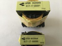
Thanks all!
With the help of a more experienced diyaudio member, I managed to trace the problem to the failed KA3525A PWM.
Once the chip was replaced all voltages were present as per the schematic.
For the benefit of anyone interested, I have attached the schematic to illustrate the role and location of the KA3525A PWM in the circuit.
PLEASE HEED WARNINGS ISSUED BY OTHER MEMBERS IN PREVIOUS POSTS!
SMPS ARE DANGEROUS - AS IS ALL WORK WITH ELECTRICITY!
Attachments
Last edited:
- Home
- Design & Build
- Parts
- Mackie SRM1801 Transformer information