Hi all
just working out the wiring for a pair of Lang 20W Class A amps, and am a bit confused about the grounding.
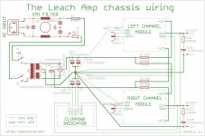
http://gdurl.com/6Rsz
The amp uses 2 supplies - 20V @ 4A (output stages) and 24V @ 100mA (low level stages). As you can see on the board layout, there is a 0v connection, and a 'T' connection. Any ideas?
thanks
just working out the wiring for a pair of Lang 20W Class A amps, and am a bit confused about the grounding.
http://gdurl.com/6Rsz
The amp uses 2 supplies - 20V @ 4A (output stages) and 24V @ 100mA (low level stages). As you can see on the board layout, there is a 0v connection, and a 'T' connection. Any ideas?
thanks
Every inter-module connection needs two wires.
Keep every two wire connection as a close coupled pair.
Twisted, or coaxial, is slightly better if the size and type of cable suits.
eg.
From power supply A you need two wires. A dual polarity PSU needs three wires, twist these as a triplet.
From power supply B you need two wires. A dual polarity PSU needs three wires, twist these as a triplet.
From Audio Source Left channel you need two wires.
From Audio Source Right channel you need two wires.
Speaker Left output needs two wires.
Speaker Right output needs two wires.
Transformer secondary to rectifier needs two wires.
Install all those two wire connections.
Now compare your assembly to the schematic and find any missing connections.
Unfortunately the PCB layout designer did not agree with this most basic philosophy.
He has provided many connections as single pads. He has forgotten that current cannot flow around a circuit unless a route is provided for the return current to go back to it's source.
Last edited:
Thanks
it's more about the connections on the circuit board - there is one marked '0v', and one marked 'T'. My understanding is that the 'T' goes to the main star ground, but the '0V' - is that for the 0V return of the low current supply, or for the signal ground?
it's more about the connections on the circuit board - there is one marked '0v', and one marked 'T'. My understanding is that the 'T' goes to the main star ground, but the '0V' - is that for the 0V return of the low current supply, or for the signal ground?
post4 is wrong. Pavouk.org got it completely wrong and AJT should never have copied it. He has been told before and chooses to post this erroneous layout yet again.
Never take your audio ground to the main charging node between the smoothing capacitors ! NEVER !
Never take your audio ground to the main charging node between the smoothing capacitors ! NEVER !
The problem is that there does not appear to be a signal ground connection on the board. Unless, as I said, that is the '0V' connection pin near the output transistors, which seems a bit odd.
Never take your audio ground to the main charging node between the smoothing capacitors ! NEVER !
never use the power supply ground return wire to run your signal grounds, use a separate wire....
run those wires separately to the psu common or zero point...
post4 is wrong. Pavouk.org got it completely wrong and AJT should never have copied it. He has been told before and chooses to post this erroneous layout yet again.
Never take your audio ground to the main charging node between the smoothing capacitors ! NEVER !
Many will disagree with you on that. The input gets it's return own path to the star ground. What's wrong with that?
You need to do a bit of reverse engineering comparing the schematic to the layout to find the best place to tap into the return part of the circuit, for least interference.The problem is that there does not appear to be a signal ground connection on the board. Unless, as I said, that is the '0V' connection pin near the output transistors, which seems a bit odd.
That will not be easy.
i have been using that layout even before Pavouk published it, as early as the early 90's
it works for me, no reason it will not work for others....
nothing is....
the speaker negative or return wires go back to the star....
never use one wire for the two channels, run them using separate wires,
i never run speaker grounds to the board and then to the starr,
i use separate wires....
so you seem in the schematics there may be fewer lines,
but in the actual buildm there are more wires than the schematic called for....
it works for me, no reason it will not work for others....
That will not be easy.
nothing is....
the speaker negative or return wires go back to the star....
never use one wire for the two channels, run them using separate wires,
i never run speaker grounds to the board and then to the starr,
i use separate wires....
so you seem in the schematics there may be fewer lines,
but in the actual buildm there are more wires than the schematic called for....
Are you disagreeing or stating the opinion of other Members?Many will disagree with you on that. The input gets it's return own path to the star ground. What's wrong with that?
The charging node in between the smoothing capacitors passes enormous pulsing currents. That is the second worst place to take your main audio ground to for a reference voltage. The worst place would be the centre tap between the two Secondaries. Except there is an even worse location. Taking the Main audio ground to the chassis where the centre tap is also connected.
Many others are now confirming that the Main Audio Ground (MAG) should be located separately from the PSU common node. Then attach a voltage reference wire/trace from MAG to PSU Zero volts. This voltage reference connection can be short, or long. But it must be a finite length.
I prefer to locate the MAG at the power amplifier. I try to locate it at the centroid between the Speaker Return terminal, the Signal Return terminal and the PCB Power decoupling ground. It helps if these are fairly close to each other. This implies that the MAG for each channel is separate from the MAG of any other channel.
Last edited:
he charging node in between the smoothing capacitors passes enormous pulsing currents.
no......why call it ground then?
that point i ground zero......
Andrew'a preference is not Tony's preference....simple as that...
Are you disagreeing or stating the opinion of other Members?
The charging node in between the smoothing capacitors passes enormous pulsing currents. That is the second worst place to take your main audio ground to for a reference voltage. The worst place would be the centre tap between the two Secondaries. Except there is an even worse location. Taking the Main audio ground to the chassis where the centre tap is also connected.
Many others are now confirming that the Main Audio Ground (MAG) should be located separately from the PSU common node. Then attach a voltage reference wire/trace from MAG to PSU Zero volts. This voltage reference connection can be short, or long. But it must be a finite length.
I prefer to locate the MAG at the power amplifier. I try to locate it at the centroid between the Speaker Return terminal, the Signal Return terminal, The PCB Power decoupling ground. It helps if these are fairly close to each other. This implies that the MAG for each channel is separate from the MAG of any other channel.
Sorry, I didn't realize you were nit picking about how the star ground was drawn. using just about any decent power supply board negates the issue.
The charging node in between the smoothing capacitors passes enormous pulsing currents.
? are you denying that the charging currents pass through the PSU common node between the smoothing capacitors?no...
I did not call it ground....why call it ground then?
PSU Zero Volts would be an unambiguous term. But it's certainly not "ground zero".that point i ground zero......
We can have different preferences. But recommending a bad layout does no new Member any favours.Andrew'a preference is not Tony's preference....simple as that...
a drawing is just an idea, what matters in the end is how the amp was implemented...
i am never excited about drawings, but how the amps was actually built....
i am never excited about drawings, but how the amps was actually built....
post5 follows post4. Post5 references post4 in the reply.Sorry, I didn't realize .............how the star ground was drawn. .............
then AnhdrewT, show us a picture of you completed amp showing how you actually did your amp,,,if you want to help newbies, pictures will help immensely...
talk is cheap, only an acutal amp will show for sure....
talk is cheap, only an acutal amp will show for sure....
Here is the circuit diagram:
An externally hosted image should be here but it was not working when we last tested it.
- Status
- Not open for further replies.
- Home
- Amplifiers
- Solid State
- Grounding question