I use this device in my commercial preamp. You can’t feed it from a high source impedance because the bias currents cause output offsets. I buffered the input stage with an opamp and fed the TPA from a 47 ohm source. The offset is a few mV worst case.
Hello,
The output of these audio interfaces are not really high impedance. The Konnekt 8 I use mainly is 100 Ohm, the Scarlett 2i2 is 430 Ohm, I would not consider "high impedance". Also, both DC coupled.
I understand that it could be more universal with an input buffer, but if not needed, I do not want to add opamp at all.
Regards,
JG
Don't even bother. I tried to steer him into the right direction early in this thread and he apparently ignored every suggestion.
Hey, this is not the right voice here. It is your opinion, while you do not understand the situation. Saying something "the right direction" is not correct. I do not care as long as I prove myself I'm right.
I appreciate suggestions, yours also, but do not switch to be prophet if you do not see your suggestion followed.
JG
You appreciate suggestions, I don't understand the situation and I don't use the right voice. Yeah sure 
You should rename the thread to "how not to implement TPA6120A2". That would be much closer to reality than the current title. Other alternative titles include "how to disregard most of the manufacturer recommendations" or "how to maximise unwanted parasitics".
You should rename the thread to "how not to implement TPA6120A2". That would be much closer to reality than the current title. Other alternative titles include "how to disregard most of the manufacturer recommendations" or "how to maximise unwanted parasitics".
Look. I've dropped the DAC board as I mentioned. Now I feed from commercial audio interfaces (TC Audio Konnekt 8 mainly) which has low output impedance and DC coupling. Transformer output should be a problem, but these are dc coupled, can feed the needed bias current easy.
You believe or not, I do appreciate your first comments and considered it, than realized the opamp is not needed in my case.
I do no understand why you write like this. Also, "unwanted parasitics", what are you talking about? You spot something on the layout? Than tell me, not just throwing in unfounded opinions.
Anyway, I've finished building the compact version and I'm happy to realize the semi surface mounted PSU works just like the original full TH version :- ) That "superreg" psu is interesing. Clearly above an LM317/337 based PSU.
I will continue here for whom asked me to do. Unfortunately, I've also realized some hole size are wrong, the mains connection for example, too small. I will recreate the gerbers and resend.
JG
TPA6120A2 tab and pins should be connected to ground plane. Without PCB as heat sink chip would overheat easily. I don't know why you have huge hole there.
All traces are rather thin in my opinion.
Decoupling capacitors are quite far from chip, there will be a bit of inductance from long and narrow traces.
Removing ground plane below inverting pin is good idea as it decreases parasitic capacitance.
All traces are rather thin in my opinion.
Decoupling capacitors are quite far from chip, there will be a bit of inductance from long and narrow traces.
Removing ground plane below inverting pin is good idea as it decreases parasitic capacitance.
Hello,
The hole is to be filled, and filled already with solder. First I wet the bottom of the ic, than continue to fill the hole, this way it conducts heat better than a lot of via-s. On the other hand, the reason for this solution is not that it conducts heat better, but because I do not do reflow soldering at home.
Yes, traces are thin, I know the ideal is around 2mm, but there is no space for that. From sound point of view, it could be more wide still yes. I may change that on the PSU later, because I want to try that psu for DACs.
I did tried to put the feedback resistors right on the pins and moved the decoupling caps a bit away. It may be wrong, but I know from sound point of view the devider to the invering input is very important. That was the logic behind, it may be wrong. 47Lab did put that resistor right on the chip legs and I was told it plays important role.
I could have put the decoupling on the other side.
Thanks!
JG
What makes you think a blob of tin conducts heat better than a grid of small copper holes?
The small copper holes are not copper holes, only copper plated holes. IPC Class I and II plated through holes require an average thickness of 20 microns. This means even you put a lot of vias under that, that material is mostly FR4, not copper ... unless, you fill the vias with soldering material. So, even copper would have better heat conductivity (I guess it has, but not sure), the amount of copper there is quite little. The big filled hole will conduct better. On the other hand, the reason for the big hole is not to have better heat conductivity. The vias would give plenty comparing to the dissipated power. The reason is, for the vias, I would need to apply paste correctly for proper soldering. I just hand solder this, not reflow. This hole is easy with hand soldering. You just solder from the bottom, wet the chip bottom first, than the hole and fill it. I've used it successfully with Analog Devices DDS chips often which did produced quite an amount of heat.
Regards,
JG
It is my understanding that people have been using this approach not for better thermal conductivity but for greater ease of assembly.
Right. The amount of metal there is not needed at all. The point is, it is easy to hand solder it.
Regards,
JG
The solder blob should work. I soldered one yesterday in QFN version, that allows a better layout, but it needs hot air.
However the power and decoupling layout is just bad. Two 100nF caps on the chip and the actual large caps are a mile away.
Well, depends what you compare it to and what you optimize to. Calling this few mm "mile away" is a bit extreme. I've choosed to put the feedback resistor close, like 47Labs do. Sure I could put the caps under the IC easy, but I just did not and the result is awesome anyway. I understand it is normally the guideline, but it seems it this length does not count yet. On the other hand, I have to note, I only use 180 Ohm + headphones. A 16 Ohm headphone would require higher transient currents and may be different. I do not think this copper length would be a problem with 16 Ohm headphones either, but I have no experience with that.
Regards, JG
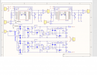
I looked at a schematic from another member but it doesn't appear to have the recommended In+ connection to ground with 4k ohm resistor TI suggests. Would this schematic work with a input transformer? I plan to run mono psu for each chip, and I intend to drive balanced Hifiman 25ohm 91db cans. I just added some resistors as an example to the earlier published shematic for illustration.. I also read that the 10 ohms output resistors could be replaced by a 300nH air core inductor, or is this only possible with the composite feedback circuit? Any insight would be appreciated!
Attachments
Hello,
You are right, I've soldered on the input pins on my pcba, but added on the pcba design beside other requests I had. I attach the current version. The modifications are minimal and straight forward, however, I have to tell I did not built this version.
I do not recommend running it from a transformer, this ic needs significant bias current. It works perfectly from low impedance DC coupled outputs.
Also, I'm afraid low output impedance is not its strength. I'm using it with a 180 Ohm and a 300 Ohm headphone. Never tested it with low imp. headphones.
Regards,
JG
Attachments
I use a dac with a lot of drive and and quite large coupling transformers with 800ohms load on the secondary at the moment. The only thing that could be problematic is if the dc current is enough to saturate the secondary winding, or does it go straight trough the 1k resistor to ground? If both Lin and Rin is at the same potential I would think no current would go through the secondary? Another member here had a composite amp with a output inductor to make the chip less sensitive to wire capacitance. That seems like an awesome solution if it works..
Also, I'm afraid low output impedance is not its strength. I'm using it with a 180 Ohm and a 300 Ohm headphone. Never tested it with low imp. headphones.
I agree. Measurements say it is OK down to 150 Ohms. HD starts climbing quickly at lower loads.
I can not comment on the output inductor. Never saw it with this IC. I'm not sure what you say on saturating the secondary winding. You mean you want to bias the transformer, so it does not go through zero crossing? That is normally done on the primary.
I'm afraid you do not pick the optimum circuit for your task. For me, after a low impedance balanced output audio interface, to higher impedance headphone in balanced config, it performs really well. I would not pick it for a low impedance headphone with transformer source. In this case I would look at something like a CK2III or b22.
This is IC is designed to drive long twisted pair balanced data communication lines, like xDSL, not low impedance loads.
JG
This is IC is designed to drive long twisted pair balanced data communication lines, like xDSL, not low impedance loads.
It is specified for 400mA into 25 ohm load, so the output stage should be pretty strong... but that's in class AB of course.
Maybe a current source at the output would help? Running a headphone amp in class A won't cost much in electricity.
Calling this few mm "mile away" is a bit extreme.
I was talking about the caps on the regulator board.
- Home
- Amplifiers
- Headphone Systems
- How to get the best out from a (or 2) TPA6120A2