The point is to lowpass (!) filter the DC bias voltage with the first R + C, then the second R provides a high enough input impedance.But why not put the high pass before the DC bias is introduced to filter out low frequency noise at the point of input from the AC signal? As it has been a while since I got involved with analog circuits, I am just trying to understand as much as I can, so forgive the repetitive questions.\\At the very least, you misinterpreted what I wrote there. Connect C1 between R3 and R4 instead.
As you were simulating it, your circuit did not make any sense, since you were running the audio signal to be buffered through that same (~1 Hz) lowpass.
Or plan B, convert the existing circuit to a negative supply.If you're concerned about PSRR then put the current source (I'd use a discrete one for lower capacitance) to the +ve rail and swap the FET for a P-channel one. Then the whole circuit draws a constant current, irrespective of signal.
Last edited:
The point is to lowpass (!) filter the DC bias voltage with the first R + C, then the second R provides a high enough input impedance.
As you were simulating it, your circuit did not make any sense, since you were running the audio signal to be buffered through that same (~1 Hz) lowpass.
Or plan B, convert the existing circuit to a negative supply.
Seems like this circuit has everything you suggested. However, when I tried applying the negative voltage, I have issues again. What do you think of the positive voltage results? What should the circuit look like for the "Negative Nelly" PSU you mentioned in a previous thread?
If you're concerned about PSRR then put the current source (I'd use a discrete one for lower capacitance) to the +ve rail and swap the FET for a P-channel one. Then the whole circuit draws a constant current, irrespective of signal.
Can you help show me how that would be implemented and what simulations I would run to verify that result? Again, new to some of the finer points of understanding audio amplifiers so any general guidance is also welcome.


Attachments
Last edited:
Positive supply and negative supply versions.
Distortion - run .tran and FFT V(out) (65536, Kaisel-Bessel window, beta = 20), use cursors to show difference between fundamental and harmonics. (H2 -56 dB, H3 -79 dB, ...)
PSRR - uncomment .ac and run that, again plot V(out).
Transfer function - swap V1 and V2 AC 1. for AC 0 and vice versa.
The "Negative Nelly" version simulates with PSRR >100 dB at 100 Hz if you increase R2 back to 100k.
EDIT: v2 fixes polar electrolytic symbol. Others are also reversed but have a nonpolar symbol so I didn't have to change anything there.
Attachments
Last edited:
Positive supply and negative supply versions.
Distortion - run .tran and FFT V(out) (65536, Kaisel-Bessel window, beta = 20), use cursors to show difference between fundamental and harmonics. (H2 -56 dB, H3 -79 dB, ...)
PSRR - uncomment .ac and run that, again plot V(out).
Transfer function - swap V1 and V2 AC 1. for AC 0 and vice versa.
The "Negative Nelly" version simulates with PSRR >100 dB at 100 Hz if you increase R2 back to 100k.
EDIT: v2 fixes polar electrolytic symbol. Others are also reversed but have a nonpolar symbol so I didn't have to change anything there.
I think this the negative v2 will be my as built version.

Can you walk me through why you made the design choices you made versus what I put together? Also, will my 12-0-12 be able to handle this? Where do you measure total power drawn? What is my range of headphone options based on either of these circuits?
The only major change is the input biasing. With a simple 2 resistor arrangement between Vcc and ground you are depending on the ratio of source impedance and bias resistor values for PSRR, which in sum isn't all that great (20-30 dB range). So I augmented the bias pot with an additional 100k - 10µ lowpass, plus another 100k for a decently high input impedance and further increased PSRR. Both measures clean up bias supply to the point where other components become the bottleneck.Can you walk me through why you made the design choices you made versus what I put together?
Depends on how big the xmfr is and how much current you need. A 12-0-12 is good for raw DC output of about 30V= with both windings in series or 15 V= with them in parallel.Also, will my 12-0-12 be able to handle this?
Hover over the Vcc source after simulating to display its "power dissipation".Where do you measure total power drawn?
Limited. You could use 20-24 V regulated with 125 mA of follower current for good results with medium to high impedance headphones (say, 100-600 ohms). In the 32 ohm range I would prefer higher current, like 250 mA, and would tend to go with paralleled secondaries and maybe 12 V regulated.What is my range of headphone options based on either of these circuits?
I've fixed / tweaked your LM317 supply - attached. Unfortunately the stock LTspice library does not seem to include an LM337 counterpart, otherwise I would have thrown together a negative supply as well. Perhaps you could make use of a premanufactured LM317/337 split power supply board and reshuffle things on the input side (transformer / rectifier) for single supply as needed.
Attachments
The only major change is the input biasing. With a simple 2 resistor arrangement between Vcc and ground you are depending on the ratio of source impedance and bias resistor values for PSRR, which in sum isn't all that great (20-30 dB range). So I augmented the bias pot with an additional 100k - 10µ lowpass, plus another 100k for a decently high input impedance and further increased PSRR. Both measures clean up bias supply to the point where other components become the bottleneck.
Basically the suppress the power supply current going into the bias and thus filtering out as much of the noise as you can?
Depends on how big the xmfr is and how much current you need. A 12-0-12 is good for raw DC output of about 30V= with both windings in series or 15 V= with them in parallel.
Hover over the Vcc source after simulating to display its "power dissipation".
Based on simulating circuits, from what I have learned so far, This circuit for a left and right headphone will pull a total of a little over 10W total with your 250 mA bias and 5W total on the 125 mA based on the "power dissipation" when I click. This should be because the out put P = I * V, which in this case I goes from 125 mA to 250 mA, so double the watts, correct? Why can my 12-0-12 transformer rated at 2A not handle this given that 24V*2A = about 48VA? I know some power is lost thermally, but I want to know more about where all the power is going I suppose.
Limited. You could use 20-24 V regulated with 125 mA of follower current for good results with medium to high impedance headphones (say, 100-600 ohms). In the 32 ohm range I would prefer higher current, like 250 mA, and would tend to go with paralleled secondaries and maybe 12 V regulated.
What would that look like? Also, what do I lost in terms of performance by running with a 12V supply instead of 20V?
I've fixed / tweaked your LM317 supply - attached. Unfortunately the stock LTspice library does not seem to include an LM337 counterpart, otherwise I would have thrown together a negative supply as well. Perhaps you could make use of a premanufactured LM317/337 split power supply board and reshuffle things on the input side (transformer / rectifier) for single supply as needed.
So this new PSU is simulating me running 20V regulated out to send 250mA of bias? Do you have a suggested design for running with lower impedance headphones? Is the reason for this issue that since P = I²R, by making R be much lower, that I need to increase the supplied current?

Is there a way for me to give up some PSRR performance in exchange for more bias? Why do I need to boost the bias for lower impedance headphones? I guess I follow most of the concepts at their base level as far as the ideas behind tweaking the bias, gate voltage, drain-to-source voltage, etc. but I am still getting my arms around it. What I would like to put together is the best performing amplifier I can using
1.) An easily available MOSFET (preferably 510 since I have been running with that so far)
2.) The transformer I already had laying around
3.) Grado S80e headphones since they are very good bang for the buck and I like all the reviews I have seen
4.) Negative supply power after reading some interesting threads regarding the topic
5.) A circuit that can be built using few(ish) parts on protoboard or something of the like.
You have been so helpful! I hope others can find a good solid beginner, budget friendly project out of this with a final build when I am done.
Last edited:
Why do I need to boost the bias for lower impedance headphones?
With a no-global-feedback design such as this, transconductance is king. Transconductance is sometimes termed 'gm' or 'Yfs' on datasheets and its a metric which determines the output impedance and also determines how much distortion is going to occur with a given load impedance.
For a source follower circuit, the output impedance is roughly 1/gm but seeing as the gm varies with drain current, a higher gm gives lower distortion. A higher load impedance also gives lower distortion as the distortion is proportional to the ratio of output impedance to load impedance. High load impedance coupled with low output impedance is the recipe for best performance in distortion terms.
Given gm improves at higher drain currents, to maintain similar distortion its necessary to run at higher bias levels when lower impedance loads are used. For a FET, unlike with a bipolar transistor, there's no downside (other than heat) for running at a higher bias level. The trouble is - most MOSFET datasheets don't show gm values at the bias levels you're likely to want in a typical headamp - which is in the hundreds of mA range. If they show gm its often at a much higher current, very few FETs indeed have plots of gm which go down to hundreds of mA.
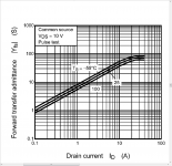
I've attached a plot of one of the very small minority of FETs which does give data in this region - to my eyes it looks a good choice based on this plot and its not expensive. Trouble is its in SMT which makes mounting on a suitable heatsink not so straightforward. Its a Toshiba TK40P03 - from the plot you can see if you ran at 250mA bias you'd be in the region of gm ~2S which translates to 0.5ohm Zout.
Attachments
Last edited:
With a no-global-feedback design such as this, transconductance is king. Transconductance is sometimes termed 'gm' or 'Yfs' on datasheets and its a metric which determines the output impedance and also determines how much distortion is going to occur with a given load impedance.
For a source follower circuit, the output impedance is roughly 1/gm but seeing as the gm varies with drain current, a higher gm gives lower distortion. A higher load impedance also gives lower distortion as the distortion is proportional to the ratio of output impedance to load impedance. High load impedance coupled with low output impedance is the recipe for best performance in distortion terms.
Given gm improves at higher drain currents, to maintain similar distortion its necessary to run at higher bias levels when lower impedance loads are used. For a FET, unlike with a bipolar transistor, there's no downside (other than heat) for running at a higher bias level. The trouble is - most MOSFET datasheets don't show gm values at the bias levels you're likely to want in a typical headamp - which is in the hundreds of mA range. If they show gm its often at a much higher current, very few FETs indeed have plots of gm which go down to hundreds of mA.
I've attached a plot of one of the very small minority of FETs which does give data in this region - to my eyes it looks a good choice based on this plot and its not expensive. Trouble is its in SMT which makes mounting on a suitable heatsink not so straightforward. Its a Toshiba TK40P03 - from the plot you can see if you ran at 250mA bias you'd be in the region of gm ~2S which translates to 0.5ohm Zout.
Super interesting. Do you have any papers or YouTube videos or even other posts on here that dig in to the weeds of some of that? Also, can you maybe comment on the effects of dropping drain voltage in favor of higher bias current? Or whether my 12-0-12 2A transformer could be pushed to feed a 250 mA bias based on the concerns addressed below? I am now leaning towards these headphones, which I think would be the easiest way out of this constraint. Pushing these with the last PSU posted should not be an issue from what I can tell. I would like to continue the discussion, but I think will be my final builds are attached. Let me know your thoughts.
beyerdynamic DT 990 PRO: Open studio monitoring headphones
The only major change is the input biasing. With a simple 2 resistor arrangement between Vcc and ground you are depending on the ratio of source impedance and bias resistor values for PSRR, which in sum isn't all that great (20-30 dB range). So I augmented the bias pot with an additional 100k - 10µ lowpass, plus another 100k for a decently high input impedance and further increased PSRR. Both measures clean up bias supply to the point where other components become the bottleneck.
Depends on how big the xmfr is and how much current you need. A 12-0-12 is good for raw DC output of about 30V= with both windings in series or 15 V= with them in parallel.
Hover over the Vcc source after simulating to display its "power dissipation".
Limited. You could use 20-24 V regulated with 125 mA of follower current for good results with medium to high impedance headphones (say, 100-600 ohms). In the 32 ohm range I would prefer higher current, like 250 mA, and would tend to go with paralleled secondaries and maybe 12 V regulated.
Also, I see now when I measure the power dissapation at the actual transformer that chasing down 250mA of bias yields dangerously close to 50W being pulled, but where is that all going to? And I still am wondering how the trade off between lower Vds and higher bias current all works together?
I'm really excited to start this build.

Attachments
Super interesting. Do you have any papers or YouTube videos or even other posts on here that dig in to the weeds of some of that?
I got started down the rabbit hole of FET transconductance from reading this Bob Cordell paper from many decades back. Although its about a classAB speaker amp it contains plenty of technical background pertaining to MOSFET characteristics which is applicable to your application.
http://www.cordellaudio.com/papers/MOSFET_Power_Amp.pdf
Also, can you maybe comment on the effects of dropping drain voltage in favor of higher bias current?
In my limited experience, dropping the drain voltage is dependent on source impedance. If your source impedance is low enough you don't have to worry about the highly non-linear Cgd introducing distortion. Cgd goes up rapidly with lower Vgd so it pays to keep enough volts there if you've not got low source impedance. Alternatively there is always bootstrapping the drain.
I got started down the rabbit hole of FET transconductance from reading this Bob Cordell paper from many decades back. Although its about a classAB speaker amp it contains plenty of technical background pertaining to MOSFET characteristics which is applicable to your application.
http://www.cordellaudio.com/papers/MOSFET_Power_Amp.pdf
In my limited experience, dropping the drain voltage is dependent on source impedance. If your source impedance is low enough you don't have to worry about the highly non-linear Cgd introducing distortion. Cgd goes up rapidly with lower Vgd so it pays to keep enough volts there if you've not got low source impedance. Alternatively there is always bootstrapping the drain.
Thanks for that reference. Given that while putting out 250mA of bias, my transformer shows total output of almost 50W

Do you think the transformer will be able to handle that kind of load? I know I can set the bias to 125mA, but that is x 2 because of left and right channel correct?
Looks to me like you've not yet taken up my recommendation to set your transformer primary inductance to 100H. So the currents will be orders of magnitudes too high on the primary side leading to excessive losses.
My fault. I am trying to keep up with everything and update the circuit as I go, but I forgot to include your changes. The results I am getting now don't really make sense though. All I did was copy the ratio with the primary being 100H as you said.

It seems to work much better with 1 H / 10 mH for me, too.
Looks like the coupling factor K is at fault. If you set this to 1, everything's honky dory. So what have we learned - for super high inductance, you need super good coupling, too. (So probably things wound on top of each other. Then you may get a problem with pri-sec capacitive coupling, so a shield winding may be called for as well.) Which, together with the inevitable winding losses, may help explain why transformer designers may choose to accept some saturation (and resulting losses) for better power output.
Re: the whole transconductance subject again, think of it as fundamentally related to impedance (which it is - output impedance of a follower is dominated by 1/gm). If you want the same power in a lower impedance, you need higher current and lower voltage: P = V²/R = RI² == const.
So if you want to drive 32 ohms instead of 128 ohms (so 1/4 the impedance), you'll need half the voltage but twice the current, with the ratio of both now being 1/4 of what it was before. Hence why I suggested twice the idle current at half the supply voltage, including secondary windings in parallel instead of in series.
In things like tube or PA amplifiers, an output transformer with multiple secondary taps would take care of this. Not like you want any in your signal path if you can help it, transformers are pretty messy.
Last edited:
*hunky doryIf you set this to 1, everything's honky dory.
*grmbl*
It seems to work much better with 1 H / 10 mH for me, too.
Looks like the coupling factor K is at fault. If you set this to 1, everything's honky dory. So what have we learned - for super high inductance, you need super good coupling, too. (So probably things wound on top of each other. Then you may get a problem with pri-sec capacitive coupling, so a shield winding may be called for as well.) Which, together with the inevitable winding losses, may help explain why transformer designers may choose to accept some saturation (and resulting losses) for better power output.
Re: the whole transconductance subject again, think of it as fundamentally related to impedance (which it is - output impedance of a follower is dominated by 1/gm). If you want the same power in a lower impedance, you need higher current and lower voltage: P = V²/R = RI² == const.
So if you want to drive 32 ohms instead of 128 ohms (so 1/4 the impedance), you'll need half the voltage but twice the current, with the ratio of both now being 1/4 of what it was before. Hence why I suggested twice the idle current at half the supply voltage, including secondary windings in parallel instead of in series.
In things like tube or PA amplifiers, an output transformer with multiple secondary taps would take care of this. Not like you want any in your signal path if you can help it, transformers are pretty messy.
That all makes sense. Given the configuration I am looking at, I guess would you be able to walk me through picking a bias based on the datasheet for a IRF510? I am reading about MOSFET amplifiers and configurations but biasing using a CCS seems a little trickier.


- Status
- This old topic is closed. If you want to reopen this topic, contact a moderator using the "Report Post" button.
- Home
- Amplifiers
- Headphone Systems
- IRF610 Class A Headphone Amp