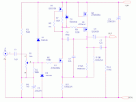
Here's how the simulation plays out. I set the currents in the sim to equal the way the actual amp is biased. The input ZVN3306A fets should be selected so that the biasing is the same for both channels. The current setting resistor on the BSS159 current source is also different than in the actual amp. This resistor wil be different for different lots of BSS159s, but very consistent within that lot. The input fet is biased at ~15 ma so that there is some current to drive the gate of the output mosfet.
In subsequent revs of this amp. I'll be inserting a pot so that the input mosfet bias current can be more easily adjusted. The output 75 ohm resistor needs to be (4) 300 ohm resistors in parallel to keep the temperature rise down. Even with two "2W" 150 ohm metal oxide resistors in parallel, the resistor temperature is around 80C, a bit high for my taste. The resistors are accordingly spaced off the board.
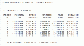
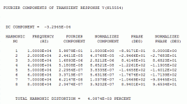
Sooner or later, I'll fire up my distortion analyzer to see how the thing really fares.
In subsequent revs of this amp. I'll be inserting a pot so that the input mosfet bias current can be more easily adjusted. The output 75 ohm resistor needs to be (4) 300 ohm resistors in parallel to keep the temperature rise down. Even with two "2W" 150 ohm metal oxide resistors in parallel, the resistor temperature is around 80C, a bit high for my taste. The resistors are accordingly spaced off the board.
Sooner or later, I'll fire up my distortion analyzer to see how the thing really fares.
Attachments
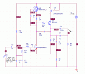
I'm also exploring the possibility of using a small-signal Darlington as the input device instead of a mosfet. This results in lower simulated distortion (higher loop gain), allows me to ditch the input protection diodes, and also makes the input stage biasing much more consistent, removing the need to select and match mosfets.
I'll most likely build up an example over the holidays, as I have a couple of extra PCBs to play with.
I'll most likely build up an example over the holidays, as I have a couple of extra PCBs to play with.

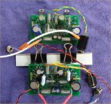
Here's pictures of the two boards - the top is the mosfet input implementation, the bottom has a Darlington input. Each board has two channels. I'm using a piece of sheet metal and some paper clamps for temporary heat sinking during testing, but the finished amp will be housed in a black anodized aluminum case that will double as heat sink.
Attachments
The darlington circuit looks even better.
Nice boards, compact.
Have you found the depletion MOSFET BSS159N for sale?
You probably have some pieces at home.
Nice boards, compact.
Have you found the depletion MOSFET BSS159N for sale?
You probably have some pieces at home.
The BSS159 is an Infineon part. Both Digi-Key and mouser have them. In a pinch, you could sub the Supertex/Diodes, Inc. part DN2530N3 and it would work just fine, but the Infineon parts have lower capacitance. The only downside of the Infineon part is that it's in a SOT-23 package. I wish they made them with legs...
Last edited:
Yes, BSS159 is a very small transistor.
I always try to use TO-92.
DN2530N3 will work just as good, you say. I believe you.
BSS159 is a part of the Multisim spice. And so are the other of your setup.
If I want to sim your circuit.
I always try to use TO-92.
DN2530N3 will work just as good, you say. I believe you.
BSS159 is a part of the Multisim spice. And so are the other of your setup.
If I want to sim your circuit.
I'm implementing some compensation changes spurred by simulation results from this morning, to get rid of a nasty peak in response at ~10 MHz. It'll be interesting to see whether the real-world simulation results from a gain-phase analyzer come close to the stuff I saw in sim.
The only questionmark I have
is the M6 ZVN3306 on top.
Why do you have that NMOS on top of the circuit?
Is it to make some space for the previous stage?
I refer to the darlington circuit.
is the M6 ZVN3306 on top.
Why do you have that NMOS on top of the circuit?
Is it to make some space for the previous stage?
I refer to the darlington circuit.
The mosfet provides a voltage drop so that the BSS159 current source is properly biased, but with a lowish incremental impedance so as not to ruin the gain of the output mosfet . I often use an LED for this purpose, but the current is too high for that here.
Here are the gain-phase plots for the latest build using a Darlington input stage and the latest compensation scheme. I'm pretty happy with the results. Schematic will follow when I get some square wave response data.
Attachments
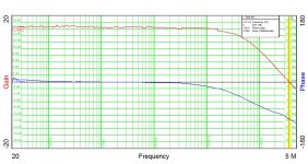
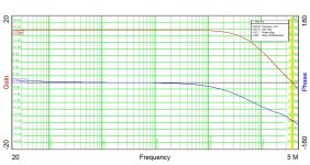

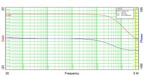
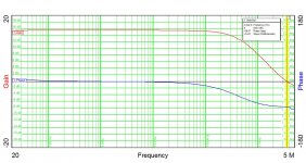
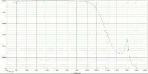
To illustrate the reason why I changed the compensation, here are two PSpice simulations in the frequency domain. The first shows the response with the original compensation scheme, showing a nasty peak at ~10MHz. The actual frequency response plot from the G-P analyzer showed the gain passing through 0dB, but there's no way of knowing if the the response peaks up again, as the analyzer I'm using only goes out to 5 MHz.
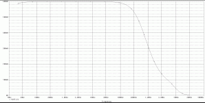
The second plot with the changed compensation as in post #16 shows the response passing through 0dB and staying there like it should - much safer in my point of view. The gain passes through 0dB at a somewhat higher frequency than in the actual scan, but the simulation doesn't account for all the stray capacitance in the actual circuit and PCB.
The second plot with the changed compensation as in post #16 shows the response passing through 0dB and staying there like it should - much safer in my point of view. The gain passes through 0dB at a somewhat higher frequency than in the actual scan, but the simulation doesn't account for all the stray capacitance in the actual circuit and PCB.
Attachments
Last edited:
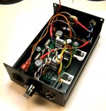
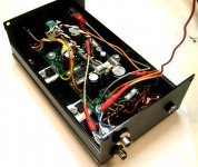
Here are some pics of the near-finished package. The innards fit into a neat little black anodized case picked up on Ebay. I'm powering the works with a little 24V/1A SMPS I picked up surplus. I used this approach rather than a linear supply, as this thing is going to India, where the line voltage is, to put it mildly - variable. Whether the SMPS will hold up under the various nasties present on the Indian grid is another question. Since the recipient runs a power supply company, he may just have access to something that will stand up to the abuse if the supplied adapter goes phhhht. I'm sending two pieces along with it just in case...
Attachments
It is not difficult to put together a discrete amplifier.Here's the latest version of the Darlington input option showing the changed compensation position.
The difficult thing is often to put in adecvate compensation.
I use Multisim AC Analysis.
Some circuits need compensation changes 10 times or more
before I am satisfied.
Some amplifiers are even impossible to reach 100% comp.
Your results with the latest comp are very good.
Good work!
I brought up the amp tonight with the aforementioned 24V switching adapter, and it sounds nice and clean, with no funny business. I installed a common mode choke right at the power input barrel connector to help filter out any common mode nastiness that might otherwise crawl down the power cable.
What's left now is tightening up and locking all the nuts and screws, dressing the interior wiring, and adding a blob or two of hot melt for mechanical stability.
The amp reveals whatever the source material has to offer, bad or good. Next up might be a vacuum state amp. I have two in mind, - one, a circuit similar to this one, but using a tube front end and transformer coupling, and a parafeed amp using a commonly available vertical oscillator/amplifier dual dissimilar triode.
- Home
- Amplifiers
- Headphone Systems
- Simple Single-Ended Headphone Amp