Trying to get a bipolar LED [Red / Green - a+c / c+a parallel - 2 lead ] or even a common cathode 'dual LED' [Red / Green - a a c+c - 3 lead] has me virtually driven to distraction now, and I must set aside due to higher priorities for a couple of weeks now.
I have a speaker protection board using uPC1237 chip.
Pin 6 of this is output to drive relay and LED indication of OK state. Rated at 80mA I think.
Pin 6 goes to ground [logic low] in OK state.
On delay O/L , DC detect or AC fail drops relay when this output is other than logic low [ground]
I have modified protection board to use MOSFET due to rated output of the mono Amp [70V Dc rails into 8 Ohm load] A relay isn't up to this load break capacity [industrial DC contactor maybe capable] - long standing subject of other threads.
In using opto driver chip for the MOSFET I discovered the initial circuit design flawed due to slow discharge or + rails on the board [12V AC in with single diode rectification and smoothing capacitor for uPC1237 and relay [opto driver supply].
Took at least 1 second for a temporary indicating LED plugged into the opto driver IC socket [as test] to dim out on a power fail or DC fault trigger. This is despite opto LED limited to 10mA at 1.3V - much lower than what the test LED would normally be fed.
The protection board [cheap built china eBay] is correct by uPC chip circuit design... the relays and indication of OK [parallel connection] fed from board + rail and both taken to ground via pin 6 - no problem as such...aside of slow.
This board is fed by a 17V winding in the main trano, so all well and good 'separate supply'.
Fixed this slow drop issue by installing a separate diode for opto supply that has no capacitor.... all well and good. so 17V AC = diode = opto = diode [reverse feed prevention] = resistor [current limit to 12mA] = pin 6 [switch to ground].
Reverse feed diode there due to board + at 21V and opto supply at +8V.
This difference in + is another mind bender issue I don't get.... why do I see only +8V / ground [1N2007]when it is fed from a 17V AC supply and the other diode has +21V / ground? Why do I measure near a 2M ohm resistance across this device tested prior to installing?
Anyhow, main problem is, I wanted to use bipolar LED to give not only ON [green] but also FAULT indication [red] in the same lamp package..... so, sounds easy enough transistor switch circuit ie. NPN and PNP setup in a variety of configurations, so I thought. NOT SO.
I get an OK but not Fault... or Fault and opto when Ok circuit removed.
I suspect trickle from transistor Base is sending opto low.
Damned if I can get this to work properly using any of the circuits I have found or even configured. What did work as transistor switched for 'fault' had the opto indicating LED partially lit when it shouldn't be like in an ON delay state.
Like I say, near driven to distraction and given up on it for now... although I'm thinking another option would be CMOS logic gate use [inverter] driven by pin 6 with pull up resistor to +ve [as used in failed transistor switch logic] to isolate opto, OK Led and Fault LED. I use the 3 lead bicolour LED.
So thats Invert = invert for opto and invert = invert for OK and invert for fault.
Been a while since I played with CMOS logic so the question is... will these handle loading like 15 - 20mA driving a LED?
Looking for a certain to work low component count solution to this problem... be it CMOS or Transistor switch logic.
Any ideas folks?
......and why that low voltage output 8V from the 1N2007 mystery... or is it high output 22V from original diode in this board?

Thanks for try.... but I only have one 'switch', being the output gate of the protection IC [pin 6 ] internally wired to ground in OK status.
Bit of a distraction tangent.... driven to distraction... but,
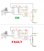
I guess there could be 4 states of indication with a 2 colour [2 or 3 pin]
Off
Red
Green
Yellow .... when both red and green driven or oscillating between R & G rapidly..... and further shades if differing proportions of R & G cycling. 10% R with 90% G = ?
Bit of a distraction tangent.... driven to distraction... but,
I guess there could be 4 states of indication with a 2 colour [2 or 3 pin]
Off
Red
Green
Yellow .... when both red and green driven or oscillating between R & G rapidly..... and further shades if differing proportions of R & G cycling. 10% R with 90% G = ?
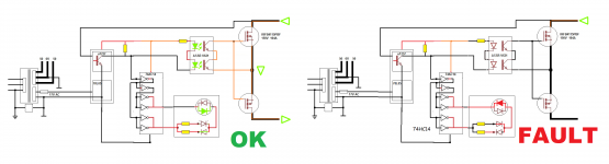
I latch the fault indication on my protection circuit, with a 74HC74. this has opposite polarity Q and not Q outputs. One has about 1 ma of drive, so the outputs will drive a PN2222 transistor. The PN2222 can drive the red and green LED's with appropriate collector resistor for the power supply. I also put in series with the green LED the photodiodes of photovoltaic NFET drivers, one for plus rail, one for minus rail. Thus green led has a lower collector resistor than red LED. The clock of 74HC74 is tied to ground. The flip flop is reset with a RC timer on power up. On fault the flip flop stays set until power off. The set of the flip flop is currently set by fault detect through an optoisolator. Various optoisolator collectors can be put in parallel on the set pin to set fault for DC on speaker for too long, heat sink overtemperature, excessive current out the speaker pin of whatever duration you want, etc. The set pin is pulled up by a resistor, the optoisolators pull it down.
The red/green 3 lead LED is stuck out the fan grill on the front so I can see it, captured by a bit of insulator board screwed to the case front. I have a separate 5 V power supply for the fault circuit, since my amp has flying ground and I also do not want to load the op amp +-16 supplies with switching functions. This allows me to use the two halves of the 74HC74 flip flop for the two different channels.
The red/green 3 lead LED is stuck out the fan grill on the front so I can see it, captured by a bit of insulator board screwed to the case front. I have a separate 5 V power supply for the fault circuit, since my amp has flying ground and I also do not want to load the op amp +-16 supplies with switching functions. This allows me to use the two halves of the 74HC74 flip flop for the two different channels.
If you use a digital logic IC to drive the LED {and indeed that is exactly what I would do, myself}, there are a few constraints that need to be met or else it'll fail and possibly catch fire
Then wire up the logic gate IC to form an H-bridge, where you drive the left end of the (LED + series resistor) with Signal, and the right end of the (LED+series resistor) with SignalBar. If you happen to select the TC4428 integrated circuit made by Microchip, this becomes especially straightforward: all you need is one single 8 pin IC, because half of it is inverting and the other half is noninverting. Nice!
- The IC's output-High current and output-Low current must both be large enough to illuminate the LED brightly. That probably means IOH>15mA and also IOL>15mA.
- You must power the IC from a constant DC voltage source that's within the IC's specification (5V for TTL, 3-15V for CMOS, 4.5V-18V for TC4428)
- The input signal you apply to the IC ("Fault/OK") must meet the I/O voltage specification of the chip. Can't apply a 30V signal to a TTL chip!
Nice example is fine by me, and small, without resorting to SMD scale.
driving transistors.... still small RE footprint. Regulated PS still fits a cramped location even with components de-rated.
Fire not nice... Principal fire concern in this has been the potential at MOSFET. Layout has Source and Drain bus wired leads to screw terminal blocks at around 4mm long and far away from any other circuit component on board [except the driver chip]. No PCP board tracks used there.
Treating this side of things as if it's high fault current 240V AC mains power wiring - as it should be.
I've got the rail nfets on a separate heat sink between rail caps & output transistor board, out in the breeze from the fan. Thin heat sink salvage from a PCAT power supply. The rail nfets have 1/4 flag terminals crimped, then soldered to source & drain, since 40 amps are normal currents in my amp (2 ohm rated, 5 pairs output transistors). The latch IC, opto driver transistors and opto fault sense are on a board somewhere else near the 5 v wall transformer for fault & LED power. Soldering the flag terminal in addition to crimp is used to allow the femtoamps from the photovoltaic fet drivers to get to source, without interruption from tin oxide over years of service. Of course gate is soldered on the Nfets. Wiring rail cap to output transistor board was 10 ga as delivered and size maintained with flag terminals, pro grade US made ones. I found ****ese flag terminals would burn off the wire at > 35 amps on the ignition switch of my car when previous owner installed electronic ignition. R**** S**** sold the worst **** parts. Changing to ideal brand flag terminals made the ignition totally reliable.
I did all this rail fet disconnect because the crowbar triac used to burn the PCB traces to itself off the board when DC on speaker happened, instead of blowing the mains breaker. The bond wire to the nfet should melt if a 1/4 phone plug to speaker is shorted again by being partially pulled out. I reused the OEM DC detect circuit that used to drive the crowbar triac, just driving an optoisolator to set the latch IC, since the two channels have flying ground and the DC detect will be at different voltage for the two channels. Optoisolators are $.63, I'm considering using four optoisolators to detect current across the rail nfets d to s and set the fault latch for that too. 50 A current causes about a 1.2 v drop. Just as the nfet heats up, voltage across nfet and sensitivity of overcurrent detect will go down.
I did all this rail fet disconnect because the crowbar triac used to burn the PCB traces to itself off the board when DC on speaker happened, instead of blowing the mains breaker. The bond wire to the nfet should melt if a 1/4 phone plug to speaker is shorted again by being partially pulled out. I reused the OEM DC detect circuit that used to drive the crowbar triac, just driving an optoisolator to set the latch IC, since the two channels have flying ground and the DC detect will be at different voltage for the two channels. Optoisolators are $.63, I'm considering using four optoisolators to detect current across the rail nfets d to s and set the fault latch for that too. 50 A current causes about a 1.2 v drop. Just as the nfet heats up, voltage across nfet and sensitivity of overcurrent detect will go down.
Last edited:
The 3rd best way to design this circuit, is to use the Advanced CMOS ("AC") line of logic ICs from Texas Instruments. They have plenty of grunt: IOH=24mA and IOL=24mA, so they can drive most panel indicator LEDs to full brightness.
The diagram below uses the hex Schmitt Trigger inverter device called SN74AC14N. Mouser.com has many of them on the shelf, ready to ship, at a low price: (link). You could down-regulate your amplifier's high voltage positive supply, to the necessary +5VDC, using a 5.6V zener diode, a MPSA42 high voltage NPN transistor, and a 20K resistor. Just be sure to connect a 100nF bypass capacitor within 0.2 inches of the AC14's VCC pin. It is a very Very fast digital chip and needs stiff supplies or else the fast transients can make it self oscillate. You don't want that.
Observe the very low parts count: one 14-pin IC, one current limiting resistor, and the LED itself. I'm deliberately not counting the +5VDC voltage regulation parts, because all of the best designs need a voltage regulator of some kind.
_
Attachments
If you redraw the circuit using the logic symbols found in Figure 1 of the attached 74AC14 datasheet, that will get you 95% of the way to the end goal: understanding what's going on. I've also attached an application note that highlights many of the reasons why Schmitt Triggers are righteous and praiseworthy. There is also this article on Wikipedia that explains Schmitt Triggers, and this video on EEVblog.
I've attached the Motorola/ON_Semi datasheet rather than the TI datasheet, because I think Motorola has drawn their Figure 1 better than TI; Motorola's datasheet makes it easier to understand what is going on, IMHO. 74AC14 ICs from Moto and from TI are perfectly compatible and perfectly interchangeable; I just happen to prefer one datasheet more than the other. Please feel free to download TI's datasheet (and also Toshiba's datasheet) if you are curious; you won't find any inconsistencies but you will find different styles of communication.
_
Attachments
Hi Guys
Food for though.
Why not take my basic circuit in #2 and remove the PNP and connect the resistor to +? LED is RED or GREEN when S1 is changed. No active parts.
Duke.")
Many helpful options here, thanks all. Some more suited to need here.
Will post circuit soon that can explain application and logic flow.
SN74AC14N is on it's way here.
Component count was important factor.
Pity not a quad rather than hex pak.
Thought here today was it's been near 30 years since I was playing with logic chips, being the 4000 series. Suspected it would be a less steep learning curve to recall than TR switch logic.
My work fields since then been at a different level to this power and control logic... more Dc relay switch logic and high kA rated at > 415, < 220kV.
Arrow stocks the quad Schmitt gate called 74AC132 and their price is very low. However this device has been discontinued by the manufacturer, and once Arrow sells their remaining stock of 9500 chips, these parts will become harder to source. Even though it's a quad not a hex, the AC132 comes in the same 14 pin package as the AC14.
A smaller-footprint design uses the TC4428 made by Microchip, which comes in an 8 pin package (either SMD or THT, your choice) and needs exactly the same external components as the 74AC14.
And the smallest-footprint design of them all, uses two Fairchild FAN3111 devices, one on the top side of the PCB and the other on the bottom side. This design needs exactly the same external components as the 74AC14 and/or the TC4428.
Design #4: "Circuit Efficiently Switches Bipolar LED", EDN magazine, Nov 22, 2001: link
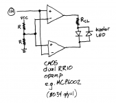
Design #5: CMOS dual opamp with Rail to Rail IO capability, figure attached. Notice this IC has 8 pins, not 14, and is cheaper than any 74AC logic chip.
_
Design #5: CMOS dual opamp with Rail to Rail IO capability, figure attached. Notice this IC has 8 pins, not 14, and is cheaper than any 74AC logic chip.
_
Attachments
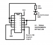
This is simplified application circuit showing u1237 'sinking trigger to drive 'relay' into ON state. amp module omitted.
With opto instead of relay coil load I was getting opto {standard LED in socket to test} dimly lit LED in an OFF state. TR circuit removed no [I suspect] trickle via Tran Base driving the damn thing.
Anyhow - 98% of the way explaining logic levels there..
So, the BiLED circuits prevail.... what about the Common Cat or Common Anode [3 lead] type?
Easy adaptable into circuit below.
But thats where I was running into trouble trying to TR drive it.. Was using NPN and PNP for each LED feed.
Attachments
Last edited:
Is there any merit in driving the MOSFET driver chip and 74AC14 from the u1237 ?
Output gate current of the 74AC14 [24mA] is 50% higher than any LED load, be that panel indicator @ 12mA or MOSFET driver at 12mA.
I don't need bright indicator level in a darkened home theater environment, so running at lower end is fine.... or if really needed run, indicator LED at 20mA, being around 75% load capability of the 74AC14 rating.
This is the reason I mention the option of a quad rather than hex chip.
It follows, what merit is there in parallel connected invert gates driving the panel indicator LED other than using these redundant outputs provided in a hex package?
I was going to raise this question with a transparent 'grey out' mask of these apparently redundant outputs in my diagram, for further discussion of circuit design principals, so thanks for raising this issue.
- Status
- This old topic is closed. If you want to reopen this topic, contact a moderator using the "Report Post" button.
- Home
- General Interest
- Everything Else
- Bipolar LED driver circuit?