I'm considering creating a spectrum analyser using this ADC7768 based development board - at 256KS/s 24bit:
https://www.mouser.co.uk/datasheet/2/609/cn0540-2256468.pdf
This seems to provide a very good starting point for an Arduino based ADC for analysis software (ie python or other) that could run via USB.
Any thoughts?
https://www.mouser.co.uk/datasheet/2/609/cn0540-2256468.pdf
This seems to provide a very good starting point for an Arduino based ADC for analysis software (ie python or other) that could run via USB.
Any thoughts?
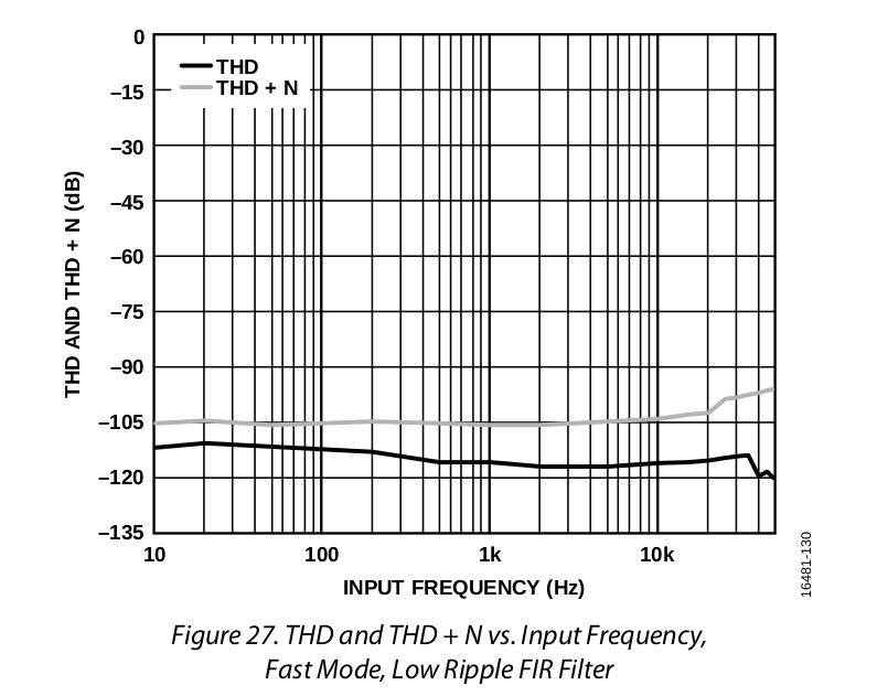
Wide bandwidth
Sinc filter bandwidth range: DC to 204 kHz
Low ripple FIR bandwidth range: DC to 110.8 kHz Precision ac and dc performance
108.5 dB dynamic range typical
−120 dB THD
±1.1 ppm of FSR INL, ±30 μV offset error, ±30 ppm of FSR
gain error
Programmable ODR, filter type, and latency
ODR values up to 1024 kSPS Linear phase digital filter options
Low ripple FIR filter: ±0.005 dB maximum pass-band ripple, dc to 102.4 kHz
Low latency sinc5 filter
Low latency sinc3 filter enabling 50 Hz/60 Hz rejection Programmable FIR filter option
So although this is a single channel version of the 8 channel 7768, the board has some hidden features:
Firstly - single and differential:

These two ports marked are the differential input, straight into the ADC.
Second - the ADC digitises from Vref- to Vref+ and in this case using a 4.096Vref chip this is a decent voltage range for the differential. The single ended has additional hardware setup to cope with up to 10V, plus has programmable offset from 0-5V.
Lastly - the maximum performance is 1024Ksps, although this depends on the digital filter used within the ADC.
The output of the DAC is serial, and from a brief scan, it's a 5byte wide frame (24bits+8bits+8bits the latter are info/padding).
The performance is a decent THD/Noise and the sampling noise (given the rate) is neatly above the audio spectrum.
The other eval boards have under side dense connector for their FPGA demo board. This is neatly broken out into pins for an Arduino. A fast enough ardiuno or chip should be able to keep up with the speed of the data transfer across to dump it onto USB for a PC to read out. Even possibly process in realtime depending on the core (thinking FFTW library).
I've also looked at this board (https://www.mouser.co.uk/ProductDet...=sGAEpiMZZMv0NwlthflBi8mdIZA2j7GuO8iwUbEl7kE=) the issue is not all the ports are exposed nicely- most go through the large connector on the underside.
Last edited:
I designed my own scope and spectrum analyser.
I used a pic32mx with separate ad9201 a2d.
I can get about 17 mega samples/second over 2 channels with that.
The PC software end did most of the business with the PIC just capturing data and sending it via USB.
It took a while to find a good FFT for the spectrum analyser with some either not working or working badly. I did find one eventually that was excellent.
I made the pc screen scalable so the traces fit the screen rather than just in a small box in the centre of the screen.

I was just reading one of the threads using an LTC2380-24. Interesting.
I've used both FFTW and an AMD GPU version of it. Surely a variant of that would provide an extremely fast processing of data? (given I've processed 54MB images in realtime using 2D DFTs)
I've used both FFTW and an AMD GPU version of it. Surely a variant of that would provide an extremely fast processing of data? (given I've processed 54MB images in realtime using 2D DFTs)
Last edited:
The LTC2380-24 thread: SAR ADC for high performance audio ADC project [LTC2380-24]
It uses the DC2289A-A demo board (https://www.mouser.co.uk/ProductDet...=sGAEpiMZZMv0NwlthflBizMwelzSOFvN4qfV8COWafA=), replaces the the clocking and adds a CPLD with a FPGA I assume.
It uses the DC2289A-A demo board (https://www.mouser.co.uk/ProductDet...=sGAEpiMZZMv0NwlthflBizMwelzSOFvN4qfV8COWafA=), replaces the the clocking and adds a CPLD with a FPGA I assume.
My work :
https://www.diyaudio.com/forums/equ...50-khz-spectrum-analyzer-diy.html#post6677918
Please, define "arduino", there are only one I know that capable to handle 24-bits SPI.
Based on this picture in DS of the ADC:
I wander why 256 ksps?
https://www.diyaudio.com/forums/equ...50-khz-spectrum-analyzer-diy.html#post6677918
Please, define "arduino", there are only one I know that capable to handle 24-bits SPI.
Based on this picture in DS of the ADC:
I wander why 256 ksps?
Attachments

The teeny 4.1 users have had SPI running at 40MHz but how reliable is unknown.
I have a couple of blackfins and a 1.5GHz arm sitting around here too. So a teeny sounds like an option however it would be consumed streaming to usb for example.
256ksps for a 1-20KHz seems good, but 192k would be possible.
That LTC simply outclasses it in terms on noise by the looks of it. Difference is the cost - 137 vs 200 for the eval board. Add 50-75 for a teeny 4.1 and other components (ie clock), so it depends on your budget.
Last edited:
My work :
https://www.diyaudio.com/forums/equ...50-khz-spectrum-analyzer-diy.html#post6677918
Please, define "arduino", there are only one I know that capable to handle 24-bits SPI.
Based on this picture in DS of the ADC:
I wander why 256 ksps?
Nice dev board - that STM controller has 32bit quadspi with DMA.
What is important to interface with PulSAR AD7982 / 3 /4 is SPI clock, to get 1msps requires 60+ MHz bus. Sigma-Delta seems not so demanding, having filtering-decimation internally. This is why I can't get 256 ksps for 54 kHz audio range - 108 should be sufficient.Nice dev board - that STM controller has 32bit quadspi with DMA.
There is new product line from Microchip - mcp3561 , $4 CAD, -120 dBc THD - though I tested at 1 kHz only so far. Max rate 153 ksps.
Sigma-Delta seems not so demanding, having filtering-decimation internally. This is why I can't get 256 ksps for 54 kHz audio range - 108 should be sufficient.
The antialiasing filter sets the bandwidth of the signal chain to 54 kHz. Piezoelectric accelerometers have bandwidths as high as 20 kHz, but a wider bandwidth signal chain has been chosen with respect to phase delay, achieving better phase matching performance in 3-axis measurements. (Further bandwidth limiting occurs in the digital filter of the ADCs, however, the phase delay is known and deterministic.)
You can upload 56 coefficients for the digital filter into the ADC - so you can tune this (and thus bandwidth) for the purpose. In the case of the eval board it's 54K for the reason the sensors and noise (reading through the documents) but that's not set in stone. You can set that separate from the rate (although the filter has some impact). The decimation for the faster filters is upto 1024ksps but the sinc3 is configurable to 256ksps.
For me - I'd like to run DC to 25.6KHz where I'm sampling 0.1 and being able to post process.
Last edited:
I'm considering creating a spectrum analyser using this ADC7768 based development board - at 256KS/s 24bit:
https://www.mouser.co.uk/datasheet/2/609/cn0540-2256468.pdf
This seems to provide a very good starting point for an Arduino based ADC for analysis software (ie python or other) that could run via USB.
Any thoughts?
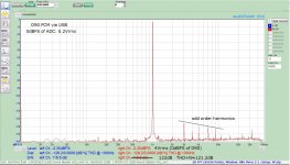
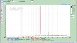
I have designed an ADC board with AD7768, where four ADCs out of eight are active. After trial and error, I gave up using eight ADCs because the THD of eight ADCs is inferior to four due to the difficulty of simultaneous driving of eight ADCs, though eight ADCs mode has better SNR. But four ADCs one has excellent results. The output is SPDIF(96kHz) or I2S(LVDS via HDMI).
Attachments
The LTC eval board is nice because you get a 300MHz MaxII 570 CPLD with EEPROM on the board (although this is there for the eval software): https://www.mouser.co.uk/datasheet/2/612/max2_mii5v1-1299433.pdf which provides options for protocol conversion (although limited). Possibly it may need some ram for packeting.
ADC -[5MBytes/sec]-> CPLD -[byte stream]-> USB IC -[USB 300MB/sec max]-> PC
I've written embedded software for USB data streaming before using cypress chips. So if the CPLD could strip data in realtime or simply forward into the USB FIFO buffer.
A USB data profile could be made to simply stream the ADC data out rather than convert to an audio digital format, simplifying the hardware needed and leaving the rest to the software.
In the past my processing stream went:
CCD -> amps -> camera ADC -[unbuffered byte read]-> Cypress USB firmware with FIFO -[USB data stream]-> Computer
Then in the computer:
USB Stream -> OpenCL buffer -[GPU buffer upload]-> OpenCL FFT -> OpenCL buffer -> OpenCL kernel programs -> OpenCL buffer to GL texture -> GL render texture to screen.
All the processing was done in GPU hence 58MB 2D FFTs done in realtime using a discrete graphics card (hence I desoldered three MBP discrete GPUs through heat 😀).
Whats the use? Electrical or acoustical?
Realtime observations or occasional "measurements"?
REW and a computer is probably a much cheaper solution... and better in many aspects.
But this one is probably more "fun" ;-D
//
Realtime observations or occasional "measurements"?
REW and a computer is probably a much cheaper solution... and better in many aspects.
But this one is probably more "fun" ;-D
//
Whats the use? Electrical or acoustical?
Realtime observations or occasional "measurements"?
REW and a computer is probably a much cheaper solution... and better in many aspects.
Audio. ... and fun 😉
Something like this could offer a hardware controlled FIFO'd parallel byte port for the CPLD: https://www.cypress.com/documentati...sb3kit-003-ez-usb-fx3-superspeed-explorer-kit
I would expect that without the hardware to support the DMA, it wouldn't keep up with a direct SPI connection to the ADC. So the CPLD would only need to convert the SPI to parallel data (I would assume 8/16/32 bit width) and handshake the FX3.
An application note here: https://www.cypress.com/file/136056/download
This shows that the interface clock is 100MHz, the cypress has a programmable hardware interface so you can create waveforms and the system will operate those on the pins in realtime (I used this for the data transfers for the camera).
Makes me wonder if, actually, the FX3 could be programmed to read SPI at the rate required for the ADC by itself 😀
In default SPI functionality, you can operate the SPI up to 33 MHz (mentioned in the datasheet).
But in case of Big-banging, you will get in the order of ~ 500 kHz.
The regular SPI clock frequency can be configured using CyU3PSpiSetConfig() function.
SPI-clock calculation: The maximum SPI clock supported is 33MHz and the minimum is 10KHz. The SPI block needs to be clocked at 2X the interface bit rate. The clock for the SPI block is derived from the system clock through a frequency divider. As the hardware only supports integer and half dividers for the frequency, the firmware uses the closest approximation to the desired bit rate.
So the answer is 33Mhz using the hardware SPI interfacing. 😢 so the only way todo high speed is through the GPIF (ie the configurable waveform interface) which has a clock rate of 100MHz. The bit-bang above is where the ARM core is toggling the signals rather than the hardware GPIF.
https://www.cypress.com/file/140296/download

Last edited:
From experience the GPIF interface does not have enough flexibility for operating a multi-command protocol SPI but could operate the SPI for a data transfer read operation. However it then makes bus sharing a nightmare for SPI for commands due to the required common bus speed. Also the FX3 has a limitation that if you use the SPI interface the GPIF can only operate at up to 16bit. However.....
The 7768 has a couple of conversion modes - including a continuous conversion, where it continues to output data until a stop 0x6C is received. So it's possible to combine conversion as 32 bit (ie using GPIF) then trigger a stop 0x6C and switch to SPI mode.
The CPLD is then connected to both the parallel byte interface and the SPI mode with an extra line for an operation mode - low for SPI and high for conversion.
The FX can then operate a command usb end point that goes via the SPI port, but if conversion is started then the operation line goes high the CPLD knows the FX3 has been reconfigured and starts a continuous conversion.
When the FX receives a stop conversion command it can then simply drop the operation line and purge the FIFO whilst then reconfiguring for SPI command mode.
This allows the system to switch between command and data acquisition without a problem without having to use a SPI read operation for each sample (and thus complexity).
So the FX3 has a small accessory board with a xylinx cool runner 128, which is about 250MHz. That should be fast enough to provide a couple of functions:
1. operation pin
transition L -> H = SPI read continuous operation
transition H -> L = SPI continue read cancel (0x6C) and connect SPI pins
2. Perform continuous read operation where it performs a serial to parallel conversion then shifts the bits into a parallel output before signalling the transfer. Although the SPI rate will be fast clockwise, the resulting parallel will be slower at 32bits wide.
In this mode there's no ack system, just keep up with the ADC.
3. SPI command req/resp rate conversion - 8bit in and 8 bit out, just reclocked. The hope here is that the internal resources of the CPLD would allow some buffering however that may not be the case. I need to look into this.
A quick check of the schematics for the CN0570 board and it shows there's a filter in place:


However that's to offset the frequency response of the ADC driver, so I think the entire talk about filters and 54Hz is a little moot.
However that's to offset the frequency response of the ADC driver, so I think the entire talk about filters and 54Hz is a little moot.
Last edited:
It took a while but the CN0540 has switchable master clocks - you have the bad RC internal (don't use), the onboard 16.384MHz YSML126W98H31 chip and the ability to connect up a separate clock. For my the onboard clock IC will be good enough.
So this is looking doable with the following:
* CN0540 demo board
* FX3 development board
* FX3 - CPLD accessory board (cool runner)
Also with the SLCK and the device being a slave SPI, it should be possible to switch SCLKing between fast and slow for the command and data modes.
So this is looking doable with the following:
* CN0540 demo board
* FX3 development board
* FX3 - CPLD accessory board (cool runner)
Also with the SLCK and the device being a slave SPI, it should be possible to switch SCLKing between fast and slow for the command and data modes.
Last edited:
With the Arduino what are you using for a display? How to control the settings? If you need a PC and the Arduino is just a digitizer its not clear to me what the benefit of the processor is over other digitizers. However I'm very interested in a stand alone FFT analyzer with display. I want to replace this: Rockland 7530A - TekWiki I have found few PC applications as easy to use or as useful as this stand alone audio frequency analyzer.
Once it’s into parallel format I think it is straightforward as the bus speed is far lower. Most micros can take parallel data via a DMA. It all depends on memory transfer performance.
A micro with fftw will work, in an a GPU would also work but most micro board have a shared memory/bus architecture but more efficient processing. The GPU need to have pixel shaders as the way a GPU FFT works is that each “pixel” of the buffer (ie each sample) is processed in parallel or more accurately queued for processing by the pool of pixel shaders.
A word of warning - GPU Floating point has been traditionally non-IEEE floating point (but almost as good), the later GPUs from nvidia have true IEEE 64bit floating support.
However it should be possible to drive a HDMI monitor. Something like Ubuntu could work (ODroid has enough peer for Ubuntu) but the key is proper hardware driver support. So I would advise something like a PI given the longer support.
Last edited:
- Home
- Design & Build
- Equipment & Tools
- Arduino Spectrum Analyser 24bit 256KS/s