Final verdict:
Don't build it with these logic chips and do it with my CPLD solution.
CPLD is very fast and accurate. I created open solution for all of you:
I2S to TDA1540 with CPLD: https://electrodac.blogspot.com/p/tutorial-how-to-programm-altera-cpld.html
Building TDA1540 from scratch: https://electrodac.blogspot.com/p/dac-ad1862-almost-tht-i2s-input-nos-r.html (look for TDA1540 section)
Hi folks,
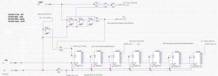
my first attempt for converting I2S to Offset Binary. This format is used in the old 14-bit R2R DAC chip TDA1540.
The conversion from I2S to Offset Binary is as simple as inverting the MSB bit. It is easier said than done 😀
My logic is created from naked logic gates and a few shift registers. It is working for the standard I2S word in length of 64 bits (generated from well known XMOS based converters, or PCM2706/7).
Basic principle:
Converting serial to parallel - inverting bit - parallel back to serial seems be hungry for parts, so I did it very simple, simple but not perfect. There is no synchronization and maybe a hidden timing issue.
Any improvements are welcome, like stop clock operation for both channels, better timing, ...
Don't build it with these logic chips and do it with my CPLD solution.
CPLD is very fast and accurate. I created open solution for all of you:
I2S to TDA1540 with CPLD: https://electrodac.blogspot.com/p/tutorial-how-to-programm-altera-cpld.html
Building TDA1540 from scratch: https://electrodac.blogspot.com/p/dac-ad1862-almost-tht-i2s-input-nos-r.html (look for TDA1540 section)
Hi folks,
The conversion from I2S to Offset Binary is as simple as inverting the MSB bit. It is easier said than done 😀
My logic is created from naked logic gates and a few shift registers. It is working for the standard I2S word in length of 64 bits (generated from well known XMOS based converters, or PCM2706/7).
Basic principle:
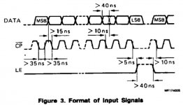
- MSB bit is inverted after each LRCK edge, controlled by XOR gate + pulse
- BCK is inverted for TDA1540, and used for shift registers for better timing
- DATA are shifted, aligned for left and right channel, latched together in 14-bits and the rest of unusable data are ignored
- LATCH is generated after each LRCK cycle
Converting serial to parallel - inverting bit - parallel back to serial seems be hungry for parts, so I did it very simple, simple but not perfect. There is no synchronization and maybe a hidden timing issue.
Any improvements are welcome, like stop clock operation for both channels, better timing, ...
Attachments
Last edited:
An experienced engineer named Nemo (from another forum) told me, that the stopped clock will be desirable because it avoids possible collisions. Digital filter SAA7030 used among with TDA1540 stopped the clock for both channels.
I can't say much about the sound because I didn't make any active comparisons yet.
I can't say much about the sound because I didn't make any active comparisons yet.
Here is the stopped clock and MSB inverter from the experienced engineer Nemo:
Far advanced design 😀 (the first one on the image is for standard I2S)
An externally hosted image should be here but it was not working when we last tested it.
Far advanced design 😀 (the first one on the image is for standard I2S)
Here is the stopped clock and MSB inverter from the experienced engineer Nemo:
An externally hosted image should be here but it was not working when we last tested it.
Far advanced design 😀 (the first one on the image is for standard I2S)
It is look a like design for Altera chip? 🙂
(BTW I am running 1540 with i2s-ST with xilinx cpld. I was amazed with 384KHz operation and 20KHz square whale out...)
This design is not working with Altera. With any cpld or fpga it has to be synchronized (from master clock), perhaps about what you did with xilinx. Nemo also has a design for synchronized CPLD (purely schema-based), but I have no right to publish it. One can find him and ask him privately.
I will test this stopped clock from basic logic elements on breadboard and if it works, I will make it as a DAC powered from USB for my collection.
I will test this stopped clock from basic logic elements on breadboard and if it works, I will make it as a DAC powered from USB for my collection.
Last edited:
Hi
I need a good function schematic for the Tda1540. Preferably i2s to Simultaneous Data 14bit.
Also i want to be able to use a saa 7030 to togle between NOS and OS (although this is something i can work on.) please help me out! I've tried everything. Kinda wanna stay on the ic side too.
I need a good function schematic for the Tda1540. Preferably i2s to Simultaneous Data 14bit.
Also i want to be able to use a saa 7030 to togle between NOS and OS (although this is something i can work on.) please help me out! I've tried everything. Kinda wanna stay on the ic side too.
I need a good function schematic for the Tda1540. Preferably i2s to Simultaneous Data 14bit.
Also i want to be able to use a saa 7030 to togle between NOS and OS (although this is something i can work on.) please help me out! I've tried everything. Kinda wanna stay on the ic side too.
From another thread:
https://www.diyaudio.com/forums/dig...e-nos-dac-using-tda1541a-586.html#post5095507
Well, Miro
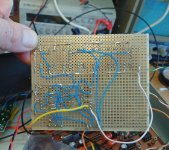
You designed it, I built it on Vero board with through hole chips and without power supply caps.
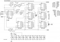
...I can confirm that your circuit works with TDA1540.
The only modification needed is that you need to take the data signal two flipflops later for both left and right (pin 6/ QD).
It took 3 hours to build, and 15 minutes of 'debugging' the flipflops number.
Congratulations, who will lay out a PCB?
You designed it, I built it on Vero board with through hole chips and without power supply caps.
...I can confirm that your circuit works with TDA1540.
The only modification needed is that you need to take the data signal two flipflops later for both left and right (pin 6/ QD).
It took 3 hours to build, and 15 minutes of 'debugging' the flipflops number.
Congratulations, who will lay out a PCB?

This is good question. It has to be compatible right now, because if you shift bits (as you did now) it should increase/decrease the bit depth. I have something for you, wait for the next post 🙂
Not sure if this works, I tested it in the past and it worked somehow, but I was dissatisfied with something there, I don't know exactly what it was 😕
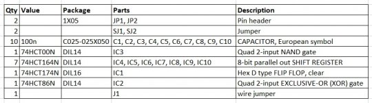
SJ1 and SJ2 are solder jumpers, you can select correct bits (for TDA1540 as you did, or perhaps TDA1541) ... take it please as untested PCB 😉
SJ1 and SJ2 are solder jumpers, you can select correct bits (for TDA1540 as you did, or perhaps TDA1541) ... take it please as untested PCB 😉
Attachments
Hi Nrik
Thanks for the report 🙂
Could You please draw the working, corrected SCH?
I am aking because I want to build and comprae to the CPLD that I am using now for the same purpose.
Thanks.
.
You could add decouplind C at each IC power pin to ground. To reduce ground bounces and maybe hear any sound difference?
Also, but if You have the scope, try to take a look at the square sygnal integrity. Should not be ringing at the edges? (prtobably have...) You can trim each contact and after that place resistor to dump ringing square edges? Usualy about 68-100 ohms. With one gate load. That gates can drive up to 15-16 next gates with 15-16X capacitance. If You have just one gate you will have ringing... Also You may like to compare the sound?
cheers
.
Contemporary USB to I2S interfaces have 32bit long "room" for data word.
What is in Your test banch before this circuit You have made?
What is in Your test banch before this circuit You have made?
- Home
- Source & Line
- Digital Line Level
- TDA1540 - I2S to Offset Binary, no CPLD, no FPGA