I have always wanted a ES9038pro main board with minimum essentials at reasonable price, with power supply and clocks open to options, so that one could try different LDO, discrete or even battery power supplies and could try different clocks and of course different analog circuits for outputs.
I searched and could not find one. So I decided to do it on my own in spare time as a fun experiment.
It is essentially just an adapter or TQFP socket, but maybe a little bit more so that one doesn't need to connect too many wires and components, better looking, and with straight-forward layouts.
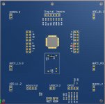
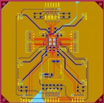
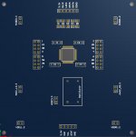
Attached are a 3D illustration of PCB that I have finished so far. Size is 10CM*10CM and can be reduced later if necessary. Nothing fancy. The circuit is pretty straight forward as provided by the factory (I might be able to post part of the schematics if the factory allows).
Right now, I am taking a short break, and want some advice before I complete the pcb design. Thanks a lot in advance.
Main features:
1) 8 channels. And of course it could be easily used as stereo or mono.
2) Dual mono with two boards.
3) All power supply open for options. I am working on a LDO regulator based on LT3045 as side project. It is easy according to LT datasheet. And there are many options available in this wonderful forum. One can even try batteries.
4) Two analog power supply (3.3V) have dedicated grounds of their own, isolated from each other and the digital ground. The digital power supplies share a digital ground.
5) Clocks can be chosen and rotated. Right now the clock with biggest footprint that I could think is full DIP14 for those TCXOs. And thus I will go with the DIP14 footprint. Other clocks can be mounted with an adapter board.
6) The digital power supplies will be bypassed and filtered on board with C0G capacitors (not shown in the PCB). Haven't decided on the analog supply bypass cap.
7) 4-layer pcb. Carefully routed so hopefully no pitfalls.
8) Hopefully it is plug and play. Power on and it can play under default setting. More settings available through external software control.
9) Relatively small size. 10cm*10cm right now and can be further reduced.
10) The board can be used for experiments and can also become part of a finished product, which means it is reasonably designed and reasonably good looking.
Advice needed:
1) Any important feature missing?
2) For analog power supply, is it much better to use film cap instead of C0G as on board bypass/filter cap? 0.1uf Film caps with reasonable size can still fit the current board size, especially if I move all the SMD components except the DAC chip to the back (the bottom layer is used as digital ground plane right now so they shall fit nicely there). ESS introduced ES9311 LDO reg and one thing they promote about ES9311 is that no bypass cap needed. And thus there might probably down side about usual bypass caps.
3) Is it a must to do isolation on the digital inputs? There are isolated usb -> I2S already.
4) How many digital input channels are considered enough? Right now I have four.
Your inputs much appreciated.
Cheers.
W. YAN
I searched and could not find one. So I decided to do it on my own in spare time as a fun experiment.
It is essentially just an adapter or TQFP socket, but maybe a little bit more so that one doesn't need to connect too many wires and components, better looking, and with straight-forward layouts.
Attached are a 3D illustration of PCB that I have finished so far. Size is 10CM*10CM and can be reduced later if necessary. Nothing fancy. The circuit is pretty straight forward as provided by the factory (I might be able to post part of the schematics if the factory allows).
Right now, I am taking a short break, and want some advice before I complete the pcb design. Thanks a lot in advance.
Main features:
1) 8 channels. And of course it could be easily used as stereo or mono.
2) Dual mono with two boards.
3) All power supply open for options. I am working on a LDO regulator based on LT3045 as side project. It is easy according to LT datasheet. And there are many options available in this wonderful forum. One can even try batteries.
4) Two analog power supply (3.3V) have dedicated grounds of their own, isolated from each other and the digital ground. The digital power supplies share a digital ground.
5) Clocks can be chosen and rotated. Right now the clock with biggest footprint that I could think is full DIP14 for those TCXOs. And thus I will go with the DIP14 footprint. Other clocks can be mounted with an adapter board.
6) The digital power supplies will be bypassed and filtered on board with C0G capacitors (not shown in the PCB). Haven't decided on the analog supply bypass cap.
7) 4-layer pcb. Carefully routed so hopefully no pitfalls.
8) Hopefully it is plug and play. Power on and it can play under default setting. More settings available through external software control.
9) Relatively small size. 10cm*10cm right now and can be further reduced.
10) The board can be used for experiments and can also become part of a finished product, which means it is reasonably designed and reasonably good looking.
Advice needed:
1) Any important feature missing?
2) For analog power supply, is it much better to use film cap instead of C0G as on board bypass/filter cap? 0.1uf Film caps with reasonable size can still fit the current board size, especially if I move all the SMD components except the DAC chip to the back (the bottom layer is used as digital ground plane right now so they shall fit nicely there). ESS introduced ES9311 LDO reg and one thing they promote about ES9311 is that no bypass cap needed. And thus there might probably down side about usual bypass caps.
3) Is it a must to do isolation on the digital inputs? There are isolated usb -> I2S already.
4) How many digital input channels are considered enough? Right now I have four.
Your inputs much appreciated.
Cheers.
W. YAN
Attachments
Last edited:
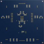
Eventually decided to move the digital ground to the third layer. So now the analog output and digital inputs traces are on top; (almost) all the power supply traces on the bottom; I2C traces are either on top or bottom or both through via depending on the ease of routing; a complete solid digital ground on the third layer; two analog ground split second layer; all SMD components on the back side (except the DAC chip) and footprints were purposely chosen to be reasonably large (1206 mostly).
A few more vias than before but I think the trade-off is reasonable. All the bypass caps and vias are close to each other and power pins. Force complete tenting on all vias.
Now that vias are unavoidable, the analog bypass caps will be through hole. Either film or ceramic caps are easily available.
Pretty much done with layouts.
Not quite sure if I need to connect the digital and analog ground planes in some way (small resistor / capacitors?). Need to read some further references.
Attachments
I'm doing a similar project, though I keep taking big breaks so my debilitating perfectionism doesn't keep me from eating. You might get more advise if you show some traces, we may also be able to spot an error.
My opinion is to pick some regulators and go by the datasheets. I'm using a mix of LT1963 and ADM7151. Both spell out requirements for minimum capacitance and ESR.
I'm excluding this on my project due to complexity/space, the fact that many USB streamers are isolated, and because the first type of signal I know I'll be using is Optical.
I go back and forth on this. If you have the room throw another header on there lesser used inputs.
Actually ESS Sabre has a document out there (If I find it I'll link to it) that advises against split planes. They don't give much in the way of reasoning but there example layouts specifically describe a single ground layer for digital and analog.
Good luck,
Brian
For analog power supply, is it much better to use film cap instead of C0G as on board bypass/filter cap?
My opinion is to pick some regulators and go by the datasheets. I'm using a mix of LT1963 and ADM7151. Both spell out requirements for minimum capacitance and ESR.
Is it a must to do isolation on the digital inputs? There are isolated usb -> I2S already.
I'm excluding this on my project due to complexity/space, the fact that many USB streamers are isolated, and because the first type of signal I know I'll be using is Optical.
How many digital input channels are considered enough? Right now I have four.
I go back and forth on this. If you have the room throw another header on there lesser used inputs.
two analog ground split second layer; Not quite sure if I need to connect the digital and analog ground planes in some way (small resistor / capacitors?). Need to read some further references.
Actually ESS Sabre has a document out there (If I find it I'll link to it) that advises against split planes. They don't give much in the way of reasoning but there example layouts specifically describe a single ground layer for digital and analog.
Good luck,
Brian
Hi, Brian,
Thanks. I found the document and attached it here. The document is talking about their demo board for ES9018 and the information about demo board can be found on ESS website.
I will post traces and some of my thoughts very soon.
Cheers.
W. YAN
Thanks. I found the document and attached it here. The document is talking about their demo board for ES9018 and the information about demo board can be found on ESS website.
I will post traces and some of my thoughts very soon.
Cheers.
W. YAN
Attachments
Hi, Brian,
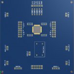
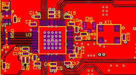
Thanks again for the inputs. Attached is a screenshot with traces. I am not completely done with the clock psu circuit yet. Need to look into different oscillator clock models before a decision can be made.
Red for top layer; deep blue for bottom layer; yellow for the second layer; and light blue for the third layer. The third layer is a whole digital ground plane. The second layer has two ground planes: left analog and right. Two ground planes divide the second layer in a way that the digital inputs and clock input traces are still riding on ground to form micro-strips.
Cheers.
WYAN
Attachments
Last edited:
Grounding
From what I read in the past few days, most articles suggesting a single ground plane for both digital and analog are based on two assumptions: either the digital section draws little current or the pcb has only two layers and component placement is a real challenge. Almost all these articles dated a long time ago. And the ESS article was for a evaluation board of two layers.
ES9038PRO draws a huge current of 400mA for the digital sections. They actually named VDD_L and VDD_R as analog which is quite against my intuition and I am still very confused. In their ES9018 schematics, ESS TECH actually put them in the category of digital.
Later articles actually advocate separate ground planes.
Staying Well Grounded | Analog Devices
For a four layer pcb, it is actually very easy, dedicate one layer to digital ground and another layer to analog ground. Don't even need to worry about partitioning one single layer, which may force some current to take a huge loop to get to the other end of the map. Two layers left are adequate for component placement.
The digital and analog ground planes might have to be connected somewhere through a diode or ferrite bead or/and a jumper -- some part of the digital circuit might have to refer to the analog ground to function properly.
There might not be any benefit of divide analog ground planes to left and right. The left(/right) analog pins are well positioned on left(/right). Associated currents do not have to cross territory if two analog channels are powered separately.
Last edited:
Hi Yan,
Interesting project.
few questions:
1. What are the plans for IV stages?
2. How does a mltichannel IV board connect to the DAC board
3. Would this work with Ian's McFIFO + multichannel USB to I2S
4. Whats are the options for programming/control the registers in 9038
5. Whats the plan for volume control?
Other considerations
Forgive my English (2nd language). I have to think and type slowly. And put stuffs in different posts so as to help clear my mind.
I have a Lampizator Big 7 for two years. Still among the better DAC I believe. In the past two years I have rotated tubes and I have always been tempted to mod this or that. After two years of fighting the temptation, instead I decide to try to build a dac from scratch. The cheap reason is that modding affect resale value, and also it is better to start fresh instead of getting deeply involved into old/existent stuffs.
So I started a R2R project based on Soekris DAM1121 which is very user friendly. Provide it with power supply and digital interface and a autoformer volume control as the simplest output stage and it is good to go. I might add one analog amplifying stage on it but I can wait.
Meanwhile I am always tempted to try dac chips as well. They are not diy friendly: you cannot solder wires to the pins and PCB has to be involved. There are a lot of register configurations to take care which is hard to decipher and their manual are not helping.
Right now, I am not sure how my DAC will look like. Feeling very insecure and that is why such a BABY-STEP project and I hope it can be done right. Hopefully it turns out to be as "plug and play" as soekris.
There are side benefits though. Designing a PCB is inevitably an effort to tie 3-dimensional components to a 2-dimensional world. A baby-step project is already a tedious task and I can imagine how involving it is going to be if power supply/out stages are also thrown in. With a main board, I can wire it to other functional module and break the 2-dimensional boundary.
Placement.
So I end up with reasonable amount of components and traces. They can be grouped into three categories. 1. Analog outputs, digital inputs and clock inputs. They are on top layer. 2. Power supplies. They are on the bottom layer. 3. Control/Register configuration related header and traces. They are on the bottom layer or the outer area of top layer. 4. Two grounds separate the components.
Digital Inputs
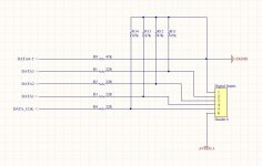
DATA4~8 pins are paralleled and pulled down to ground through a 47K resistor, per the manual instructions.
DATA_CLK and DATA1~3 are available. If the associated headers are not plugged in or no signal detected, they will be pulled down to ground automatically with a 47K resistor. 22R in the digital input line is routine.
A clean 3.3V power supply and ground is there if one wants to build a circuit of Toslink/SPDIF input with it (on another board of course) or to power the clean side of a USB interface.
The linked AD document in previous post actually hints that the clean side of digital interface might better be referred to analog ground and I will think about it. (Oscillator as well)
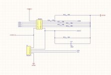
Control / Register Configuration
This is the part that I am most unsure about (though it affect the sound quality least in some sense). Like I said, the manual is hard to decipher and I might have to build or find one control module to make sure, but this is the current configuration:
GPIOs are pulled down to ground with 20K~47K resistor, but not directly. I put a jumper/header in between. When headers are shorted, GPIOs are pulled to ground; or one could instead install LEDs in between.
ADDR can be pulled up or down through jumper. Default is down.
RESET is pulled down in default. Can be pulled up through jumper (hold for long enough, and maybe a push bottom is better). For good looking I put it in a 6*2 headers.
SDA and SCL are connected to headers directly. Not pulled up or down.
I really am not sure if this setup is enough for most external control module. I will have to try. And inputs appreciated.
Attached is brief schematics about digital inputs and control.
Component Choice
Thin film resistors, C0G capacitors to decouple digital power supplies, and 4 film/c0g capacitors to decouple analog power supplies. Most of them are SMD.
Footprints for most SMD components are 1206. Good for eyes if hand soldered. There are no smaller c0g capacitors. Smaller size resistors tend to have better ppm figure but Panasonic have ERA - 8A series of resistors with 25ppm.
Any suggestions for good and neat connector/header for analog output and power supplies?
Thanks again.
Forgive my English (2nd language). I have to think and type slowly. And put stuffs in different posts so as to help clear my mind.
I have a Lampizator Big 7 for two years. Still among the better DAC I believe. In the past two years I have rotated tubes and I have always been tempted to mod this or that. After two years of fighting the temptation, instead I decide to try to build a dac from scratch. The cheap reason is that modding affect resale value, and also it is better to start fresh instead of getting deeply involved into old/existent stuffs.
So I started a R2R project based on Soekris DAM1121 which is very user friendly. Provide it with power supply and digital interface and a autoformer volume control as the simplest output stage and it is good to go. I might add one analog amplifying stage on it but I can wait.
Meanwhile I am always tempted to try dac chips as well. They are not diy friendly: you cannot solder wires to the pins and PCB has to be involved. There are a lot of register configurations to take care which is hard to decipher and their manual are not helping.
Right now, I am not sure how my DAC will look like. Feeling very insecure and that is why such a BABY-STEP project and I hope it can be done right. Hopefully it turns out to be as "plug and play" as soekris.
There are side benefits though. Designing a PCB is inevitably an effort to tie 3-dimensional components to a 2-dimensional world. A baby-step project is already a tedious task and I can imagine how involving it is going to be if power supply/out stages are also thrown in. With a main board, I can wire it to other functional module and break the 2-dimensional boundary.
Placement.
So I end up with reasonable amount of components and traces. They can be grouped into three categories. 1. Analog outputs, digital inputs and clock inputs. They are on top layer. 2. Power supplies. They are on the bottom layer. 3. Control/Register configuration related header and traces. They are on the bottom layer or the outer area of top layer. 4. Two grounds separate the components.
Digital Inputs
DATA4~8 pins are paralleled and pulled down to ground through a 47K resistor, per the manual instructions.
DATA_CLK and DATA1~3 are available. If the associated headers are not plugged in or no signal detected, they will be pulled down to ground automatically with a 47K resistor. 22R in the digital input line is routine.
A clean 3.3V power supply and ground is there if one wants to build a circuit of Toslink/SPDIF input with it (on another board of course) or to power the clean side of a USB interface.
The linked AD document in previous post actually hints that the clean side of digital interface might better be referred to analog ground and I will think about it. (Oscillator as well)
Control / Register Configuration
This is the part that I am most unsure about (though it affect the sound quality least in some sense). Like I said, the manual is hard to decipher and I might have to build or find one control module to make sure, but this is the current configuration:
GPIOs are pulled down to ground with 20K~47K resistor, but not directly. I put a jumper/header in between. When headers are shorted, GPIOs are pulled to ground; or one could instead install LEDs in between.
ADDR can be pulled up or down through jumper. Default is down.
RESET is pulled down in default. Can be pulled up through jumper (hold for long enough, and maybe a push bottom is better). For good looking I put it in a 6*2 headers.
SDA and SCL are connected to headers directly. Not pulled up or down.
I really am not sure if this setup is enough for most external control module. I will have to try. And inputs appreciated.
Attached is brief schematics about digital inputs and control.
Component Choice
Thin film resistors, C0G capacitors to decouple digital power supplies, and 4 film/c0g capacitors to decouple analog power supplies. Most of them are SMD.
Footprints for most SMD components are 1206. Good for eyes if hand soldered. There are no smaller c0g capacitors. Smaller size resistors tend to have better ppm figure but Panasonic have ERA - 8A series of resistors with 25ppm.
Any suggestions for good and neat connector/header for analog output and power supplies?
Thanks again.
Attachments
Last edited:
Hi Yan,
Interesting project.
few questions:
1. What are the plans for IV stages?
2. How does a mltichannel IV board connect to the DAC board
3. Would this work with Ian's McFIFO + multichannel USB to I2S
4. Whats are the options for programming/control the registers in 9038
5. Whats the plan for volume control?
Hi,
1. I haven't quite thought about the IV stage. I have planned to build DHT preamp for a long while and I might try to realize the plan together with the IV stage. A simple IV stage is through a resistor, and then maybe a transformer (1+1 : 1+1 or even step up) or maybe other amplifying stage. I have Lundahl LL1571XL and LL7903 that I will experiment with.
2. The main board has eight output channels and can be summed to stereo. Originally I only thought about stereo, but in pcb routing it is actually neater to keep all 8 separate channels.
3. I suppose it shall work with stereo interfaces. For multi-channel, I think it should work as well but have to double check.
4. You will have to have a standalone control module. I haven't worked on this yet. I tend to believe (or hope) that a simple arduino based module would work great but I have to look into it.
5. ES chips support a lot of functions including digital volume control. That could be realized in a control module.
By the way, for stereo, I've always preferred analog volume control. But for multi-channel digital volume control might have an edge on sound quality and certainly save big money. Cheers.
I plan to use LT3045 based regulator for the four digital power supply. The analog and clock might deserve better.
The LT3045 regulator will be squeezed in a small 13.6*30mm pcb that fits a 20*18*16 heatsink. Attached is how it is going to look "on paper". 😉
You have so much space, why not just select your regulators and build into one PCB? I know you want to experiment but I bet you will find plenty to play with regarding I/V and never hear a difference in regulators if you pick a decent setup to start.
From what I read in the past few days, most articles suggesting a single ground plane for both digital and analog are based on two assumptions: either the digital section draws little current or the pcb has only two layers and component placement is a real challenge. Almost all these articles dated a long time ago. And the ESS article was for a evaluation board of two layers.
ES9038PRO draws a huge current of 400mA for the digital sections. They actually named VDD_L and VDD_R as analog which is quite against my intuition and I am still very confused. In their ES9018 schematics, ESS TECH actually put them in the category of digital.
Later articles actually advocate separate ground planes.
Staying Well Grounded | Analog Devices
For a four layer pcb, it is actually very easy, dedicate one layer to digital ground and another layer to analog ground. Don't even need to worry about partitioning one single layer, which may force some current to take a huge loop to get to the other end of the map. Two layers left are adequate for component placement.
The digital and analog ground planes might have to be connected somewhere through a diode or ferrite bead or/and a jumper -- some part of the digital circuit might have to refer to the analog ground to function properly.
There might not be any benefit of divide analog ground planes to left and right. The left(/right) analog pins are well positioned on left(/right). Associated currents do not have to cross territory if two analog channels are powered separately.
Uh Oh. I might have to go back to the drawing board on my project then. I have a 4 layer board but I used one internal plane to distribute 5vDC to all the individual regulators.
You have so much space, why not just select your regulators and build into one PCB? I know you want to experiment but I bet you will find plenty to play with regarding I/V and never hear a difference in regulators if you pick a decent setup to start.
Hi, Thanks. It is doable, especially the four digital power supplies. There is space on the outer area. I rotate power supply modules for soekris analog supply and difference can be heard. Oscillator supplies should matter as well. I will keep options open for them for sure.
Also, putting too many power supplies onboard may have a potential heating issue.
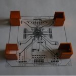
I will think about it later. Right now, I am doing a few final adjustment and will like to print out a sample first.
Uh Oh. I might have to go back to the drawing board on my project then. I have a 4 layer board but I used one internal plane to distribute 5vDC to all the individual regulators.
Have fun drawing. 🙂
For what its worth. I just finished laying out a board for this and I found it tricky. All the different power rails and the layout of the oscillator and digital I/O I found a pain. Seemed like everything was a compromise.
Not sure if this is helpful but I might:
1. I wouldn't do anything less than 4 layer for this chip. Too many power rails and digital I/O.
2. Since you have room on the board I'd think about putting on-board LT3045 or something from Analog Devices with low noise. Leave a header for a shunt regulator so it can be an OR power option. Looks like you have room for this. If the PCB area is free, seems like no harm.
3. Beef up all power lines. This is hungry IC. Thick power lines would be good.
4. Not sure if you want to make the jump to smaller by-pass caps but I put them on the same side as the IC close to the pins. 0402 fit onto the same layer as the ESS9038pro.
Looks like you got all the important stuff fairly close to the IC so it should work! Hope you have fun with this project. I put all the regulators on the bottom layer and cleared a space on the top for heatsinks just in case.
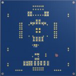
Attached is a small top layer short of what I did around the ES9038pro. I have not had a chance to get the parts on this board yet but looking forward your experiences with this.
Not sure if this is helpful but I might:
1. I wouldn't do anything less than 4 layer for this chip. Too many power rails and digital I/O.
2. Since you have room on the board I'd think about putting on-board LT3045 or something from Analog Devices with low noise. Leave a header for a shunt regulator so it can be an OR power option. Looks like you have room for this. If the PCB area is free, seems like no harm.
3. Beef up all power lines. This is hungry IC. Thick power lines would be good.
4. Not sure if you want to make the jump to smaller by-pass caps but I put them on the same side as the IC close to the pins. 0402 fit onto the same layer as the ESS9038pro.
Looks like you got all the important stuff fairly close to the IC so it should work! Hope you have fun with this project. I put all the regulators on the bottom layer and cleared a space on the top for heatsinks just in case.
Attached is a small top layer short of what I did around the ES9038pro. I have not had a chance to get the parts on this board yet but looking forward your experiences with this.
Attachments
For what its worth. I just finished laying out a board for this and I found it tricky. All the different power rails and the layout of the oscillator and digital I/O I found a pain. Seemed like everything was a compromise.
Not sure if this is helpful but I might:
1. I wouldn't do anything less than 4 layer for this chip. Too many power rails and digital I/O.
2. Since you have room on the board I'd think about putting on-board LT3045 or something from Analog Devices with low noise. Leave a header for a shunt regulator so it can be an OR power option. Looks like you have room for this. If the PCB area is free, seems like no harm.
3. Beef up all power lines. This is hungry IC. Thick power lines would be good.
4. Not sure if you want to make the jump to smaller by-pass caps but I put them on the same side as the IC close to the pins. 0402 fit onto the same layer as the ESS9038pro.
Looks like you got all the important stuff fairly close to the IC so it should work! Hope you have fun with this project. I put all the regulators on the bottom layer and cleared a space on the top for heatsinks just in case.
Attached is a small top layer short of what I did around the ES9038pro. I have not had a chance to get the parts on this board yet but looking forward your experiences with this.
Hi, thanks for the inputs. I will beef up the power lines. 🙂
For first samples, I will go with 1206. Easy to hand solder. Also, if you go with C0G capacitors, the smallest choice seem to be 1206. I put most of the capacitors on back side and there are plenty of space.
I could also put LT3045 regulators on board, but will settle on separate little power supply boards for now. Need to evaluate before further action. I know there were designs with on-board regulators that get pretty hot in working (but I check that board there are a lot of 117 regulators which tend to produce heat). Plus, I have quite some power supplies ready to try. Cheers.
Hey there, any updates on this project? Looks really cool!
Thanks a lot for the encouragement. Since there was space on board, I spent some time and integrated isolation / reclocking sub-circuit on board. These options can be disabled if the digital inputs are clean. Shall print pcb and test it soon. Cheers.
Hi there any update please? keeping my eye on this.Thanks a lot for the encouragement. Since there was space on board, I spent some time and integrated isolation / reclocking sub-circuit on board. These options can be disabled if the digital inputs are clean. Shall print pcb and test it soon. Cheers.
- Status
- Not open for further replies.
- Home
- Source & Line
- Digital Line Level
- ES9038pro main board with minimum essentials