Hi all,
I was wondering if anyone considers building the valve DAC from Linear Audio volume 13 (which is not a solid-state DAC with a valve-based output buffer, but which uses E88CC valves as the actual DAC). If so, I would be very willing to answer any questions about it. If there is more than one person who wants to build it, you can save a considerable amount of money on the main PCB by ordering it together.
Best regards,
Marcel
Edit, 18 August 2020...5 December 2024:
There are two versions discussed in this thread, the original valve DAC described in Linear Audio volume 13 and a raw DSD variant (also called the DSD-only variant) which was first built by Ray from Somerset, a.k.a. nautibuoy, and Dave who is also from the UK, a.k.a. snax (who had not finished it yet on 18 August 2020). Ray started a group buy for the raw DSD variant, see posts #481 and #661 among others: https://www.diyaudio.com/community/threads/valve-dac-from-linear-audio-volume-13.308860/post-6299387 https://www.diyaudio.com/community/threads/valve-dac-from-linear-audio-volume-13.308860/post-6311952 . An earlier attempt by leadbelly from Calgary to start a group buy for the original valve DAC did not work out, but it was restarted after the raw DSD group buy, see Interest for GB for MarcelvdG valve DAC .
Original design:
As the Linear Audio website will soon be closed, the files formerly accessible via the Linear Audio site are now attached to post #2162 with the former Editor's permission, see https://www.diyaudio.com/community/threads/valve-dac-from-linear-audio-volume-13.308860/post-7863549
For the record, when I wrote the Linear Audio article, I was under the impression that high-order single-loop sigma-delta modulators had been known since around 1990, but I later learned that Robert W. Harris already made them in the first half of the 1980's. See US patent US4509037 (application filed 1 December 1982, date of patent 2 April 1985) for details.
Raw DSD variant:
see posts #84 and #86 of this thread for the raw DSD variant, with some updated documentation in post #713.
Main differences between the variants:
Original:
-Mainly designed for PCM; generates its own sigma-delta modulates from a PCM input signal using an FPGA module and an SRC4392
-Supports DSD64 and DSD128 by first converting them to PCM
-Valve clock generator (just because I wanted to make all analogue and mixed-signal functions with valves)
-Quite expensive
Raw DSD variant:
-Designed for raw DSD; it doesn't need any FPGA or SRC4392, because the raw DSD signal is already a sigma-delta modulate
-Can support DSD64, DSD128, DSD256 and DSD512
-Gets its clock from an external solid-state clock generator and buffers it with some more solid-state circuitry
-Much less expensive
Ray uses the raw DSD version with a computer running HQPlayer, so he can use the raw DSD version and still play PCM. Basically he uses the computer to do what my FPGA board does, although the details of the used algorithms are undoubtedly not exactly the same.
Yet another approach could be to use an AK4137 board for the conversion from PCM to a sigma-delta modulate, but no-one has tried that yet. Compared to the FPGA board and SRC4392 used in the original valve DAC, it should be much cheaper, but it is also much less flexible; with the original valve DAC you can change the Verilog code and build in any filter curve you like, any sigma-delta algorithm you fancy or any amount of headroom for intersample overshoots that you want, provided you have enough knowledge of digital signal processing and Verilog code to do so.
Component value updates and known bugs and workarounds:
For both the raw DSD variant and any new builds of the original design, a couple of component values need changing:
R14, R25, R26, R27, R103, R104, R105 and R106 become 2 kohm +/- 1 %, 0.6 W metal film as otherwise the trimming range can be too small
RV1 and RV2 either stay as is (Bourns 3386P-1-502LF) or become Bourns 3296Y-1-502LF, depending on whether one prefers single or multiturn
If the trimming range should still be too small, pulling out E88CCs and putting them back in in a different order can help.
The values of C28, C29, C50 and C51 depend on what filter type is chosen. For the raw DSD variant, Ray used the filter of post #215, which requires 15 nF each for these capacitors. The filters of post #837 would require 5.1 nF instead.
There is a bug in the way the Amanero-style connector is connected in the raw DSD valve DAC (I used an obsolete Amanero datasheet). Pins 12, 14, 16, 18 and 20 of P13 (with the pin numbering as in the KiCAD schematic) should have been left open instead of being grounded. It doesn't matter when you use ppy's reclocker to drive the raw DSD valve DAC, but it does with a real Amanero Combo 384. A workaround is to remove these pins from the header/connector. See also https://www.amanero.com/drivers/combo384-D.pdf and mind the different pin numbering in the Amanero datasheet and the raw DSD valve DAC schematic.
I've caused some confusion with my laziness: for U7, U8, U9, U10 and U11 of the raw DSD valve DAC, I used 3 mm by 3 mm TSSOP-8 footprints with 0.65 mm pitch from a standard KiCad library, while the actual package type is SSOP-8, also known as SM8 or SM-8. They are compatible, but it is confusing. The TI package code in the type number is DCT.
PCB peculiarities:
The main board of the original valve DAC was designed for the Eurocircuits PCB proto four-layer PCB stack-up, which uses double layers of 180 um thick PR7628 prepreg, so in total 360 um thick prepreg. Most other PCB manufacturers use single prepreg layers by default. Although the main board of the raw DSD valve DAC was manufactured by another PCB manufacturer and although it would have been possible to adjust trace widths to get about the same characteristic impedances for the critical lines with single prepreg, we held on to the double prepreg layer because it provides a more reliable insulation than a single layer. Hence, the PCB needs a custom stack-up.
The size of the main board of the raw DSD version is 195.58 mm by 314.325 mm, the size of the main board of the original valve DAC is 264.16 mm by 328.93 mm.
Ray produced a mechanical drawing in FPD and dxf format of the main PCB of the raw DSD variant of the valve DAC, see post #751, Valve DAC from Linear Audio volume 13
0 ohm resistors and jumper settings for the raw DSD version:
For the raw DSD valve DAC, which of the 0 ohm resistors R48, R57, R58 and R59 need to be mounted and which not depends on whether one wants to use the Amanero-style input P13 and if so, whether the bit clock or the master clock is used:
P13 not used: R48, R57, R58 and R59 not mounted
P13 used with the bit clock: R48, R57 and R59 mounted, R58 not mounted
P13 used with the master clock: R48, R57 and R58 mounted, R59 not mounted
Jumpers at P8, P9 and P11:
Using the bit clock or a master clock below 25 MHz: jumper on P8, pins 1 and 2 of P9 shorted, pins 1 and 2 of P11 shorted
Using a master clock between 40 MHz and 50 MHz: no jumper on P8, pins 2 and 3 of P9 shorted, pins 2 and 3 of P11 shorted
When a master clock is used, it has to run at an integer multiple of the bit clock (an even multiple for master clocks between 40 and 50 MHz) and the data have to be stable between 5 ns before and 0 ns after the rising edge of the master clock. When the bit clock is used, the data have to be stable between 5 ns before and 0 ns after the rising edge of the bit clock.
Anything that meets the timing requirements of a DSC2 v2.5.2 also meets the timing requirements of a raw DSD valve DAC running on the bit clock.
Besides, PPY's ReClocker board as described on this website https://puredsd.ru/ in the schematic https://puredsd.ru/BBBreclk.pdf meets the timing requirements of a raw DSD valve DAC running on the master clock.
Supply currents:
The raw DSD variant draws about 1.83 A from the 6.3 V heater supply (could be a bit higher depending on the brand of E88CC), an estimated 49.05 mA from the -300 V supply and an estimated 100 mA from the 5 V supply, see posts #243 and #336 for details.
The currents are higher for the original valve DAC: theoretically 2.73 A from the heater supply (SonnyMarrow measured 3 A, see post #1641), theoretically about 75 mA from the -300 V supply (SonnyMarrow measured 67 mA) and three hundred something milliamps from the 5 V supply the last time I measured it. As this was several configuration file updates ago and as the current drawn from the 5 V supply can change when the configuration file is changed, I recommend counting on 700 mA from the 5 V supply.
For those wanting to experiment with alternative power supplies, please keep in mind that the valve DAC requires -300 V rather than +300 V and that the heater supply has to float, as it gets biased at a large negative voltage by the voltage divider R141, R140, D16, R139, R43, R47. A soft starting and stopping -300 V supply with a rate of change of 50 V/ms or less is strongly preferred to avoid stressing the 74AHCT74 chips that drive the upper E88CC valves. By the way, I've had no hum issues at all with the original valve DAC with its simple CRCRC filtered -300 V supply and AC heater supply.
Reconstruction filters:
For the reconstruction filters of his raw DSD valve DAC, Ray has used RM8 inductors from Don Audio, https://www.don-audio.com/Custom-Inductor-RM8-Core
He uses the filter schematic from post #215 of this thread, with R1 and R4 combined into a single 806 ohm resistor. He designed his own filter boards, those are also part of the group buy.
A cheaper alternative for the inductors could be to buy RM cores and to wind them manually. It's more fuss because you need to separately buy the cores, the clamps, the coil formers (bobbins) and the "enamelled" wire. The Digikey part number for the cores is either 495-76950-ND or 495-76953-1-ND and the manufacturer's (TDK's) part number either B65811J0250A048 or B65811F0250A048. The J model has no centre hole and the F version has a threaded sleeve.
When you only want to drive balanced inputs, you can use Ray's filter without the transformer and with the outputs terminated with 402 ohm resistors to ground instead of an 806 ohm resistor between the positive and negative signal lines. See post #837 for some other filter alternatives with the transformer.
The details of the reconstruction filter of the original valve DAC are in the article and database of the original valve DAC. It uses P26x16, 250 nH/turn^2, N48 potcores for the inductors.
If and only if you use an output transformer and are sure that nothing dangerous can happen when due to a fault condition, there is -350 V at its primary and 40 mA or so flowing through its primary, then there is a way to save money and reduce noise modulation as well. It involves replacing one of the DC blocking capacitors with a short and using a 100 V rated capacitor for the other. See the discussion with acg around posts #1276 ... #1279, https://www.diyaudio.com/community/threads/valve-dac-from-linear-audio-volume-13.308860/post-6484934.
For anyone wishing to redesign the filter, posts #1257, #1282 and #1300 may also be interesting.
Digital correction for the reconstruction filter roll-off:
The digital interpolation filters in the original valve DAC have a partial correction built in for the droop of the analogue reconstruction filter. No such droop compensation is possible in the raw DSD version.
Hence, for the flattest possible amplitude response, the reconstruction filter of the raw DSD version has to be flat by itself while the reconstruction filter for the original valve DAC has to have a roll-off that's about the same as the roll-off of the filter that the correction was designed for. Therefore, Butterworth filters give the flattest response for the raw DSD valve DAC and 0.05 degrees linear phase or Gaussian-to-6 dB filters give the flattest response for the original valve DAC. While the phase response of Butterworth filters is not as good as that of Gaussian-to-6 dB or 0.05 degrees linear phase filters, it is still pretty close to linear phase an octave or more below cut-off.
The digital droop correction filter has a magnitude response
1 + 13/256 - (19/512) cos(2 pi f T) - (7/512) cos(4 pi f T) with T = 5 us.
This is only a small correction: 1.009680428 or +0.083678759 dB at 15 kHz, 1.016534293 or +0.142440687 dB at 20 kHz, peak of about +0.644660534 dB at 73.5 kHz.
Output signal transformers:
The DAC is inherently a balanced circuit. I used output signal transformers to be able to connect its outputs to unbalanced as well as balanced inputs. If you only want to connect its outputs to balanced inputs, there is no need for a transformer. With reference to the filter for the raw DSD version shown in post #215, the mid point between R1 and R4 then has to be connected to ground (so you really need two 402 ohm resistors rather than one 806 ohm resistor), R2, R3, C9 and the transformer are not needed and the positive pin of the output connector has to be connected to R1, the negative pin to R4.
Also for the raw DSD version, the filter in the right schematic of post #837 is less sensitive to transformer parasitics than the one in post #215, so I recommend using the right filter of post #837 if you want to use a different signal transformer than Ray used.
Output signal level:
Neglecting transformer losses, if any, the peak output voltage is about 2.5 mA times the parallel connection of three things: the anode resistors of the upper E88CCs, together about 11.2 kohm, the termination resistor, and whatever load you get from the amplifier that's connected to the output. With an 806 ohm termination resistor and a 10 kohm amplifier input resistance, that's about 1.75 V peak or 1.24 V RMS. (This is assuming that the percentage of ones in the DSD signal varies between 25 % and 75 %, as it should according to the Scarlet Book standard.)
I do not recommend using higher impedances to boost the signal level, but using lower termination impedances to reduce the level is very well possible, provided that the reconstruction filter is redesigned accordingly and the signal transformer (if any) can handle it. If you really need a higher signal level, you can use a transformer to step it up, see the left schematic of post #837 and the text of that post.
BOMs and Digikey baskets for the raw DSD version:
See post #845, https://www.diyaudio.com/community/threads/valve-dac-from-linear-audio-volume-13.308860/post-6331624 , for lists of the components that Ray used for his build, with the component value updates included, and see post #1165, https://www.diyaudio.com/community/threads/valve-dac-from-linear-audio-volume-13.308860/post-6470605 for an update. See post #1159, https://www.diyaudio.com/community/threads/valve-dac-from-linear-audio-volume-13.308860/post-6469618 , for additional information from Periklis in Athens.
Functional checks with a makeshift lowpass filter:
A simple RC low-pass filter can come in handy for debugging the digital part of all versions of the valve DAC, see post #369 https://www.diyaudio.com/community/threads/valve-dac-from-linear-audio-volume-13.308860/post-6016188 . With a low-pass filter, a coupling capacitor, an amplifier and a loudspeaker, you can check whether a digital line that should carry a sigma-delta modulate indeed carries a sigma-delta modulate.
In the original valve DAC, there should be a suitable signal at the outputs of U11. Contrary to what I wrote in post #1533, the digital part of the original valve DAC requires the 27 MHz valve crystal oscillator and the signal indicating that the 85A2 has ignited, so it can't work without the -300 V and the heater supply.
Frequency doublers and clock subharmonics:
As the raw DSD valve DAC is quite sensitive to clock subharmonics, especially the second subharmonic (and its odd multiples) when the algorithm that generates the DSD signal is a straightforward single-bit sigma-delta modulator, I do not recommend the use of frequency doublers in the clock generation circuitry. See posts #878, #879 and #884 and post #2850 of https://www.diyaudio.com/community/...jitter-crystal-oscillator.261651/post-6373471 . If you want to use them anyway, any subharmonics have to be filtered off very thoroughly (-100 dBc would be OK, -52.75 dBc would certainly not be OK).
Noise floor:
The noise floor of the valve DAC is low enough not to bother me, but not as low as the noise of some solid-state DACs. A recording of a five-second fragment of the noise of the original valve DAC is attached to post #1428, https://www.diyaudio.com/community/threads/valve-dac-from-linear-audio-volume-13.308860/post-6521888
Neon lamps and surprise mode:
The original valve DAC has seven neon indicator lamps. (It is possible to modify the circuit and use LEDs instead.) With configuration file version 2.1 as well as all earlier versions, six of the seven neon lamps are only used for surprise mode. When SW5 is pressed, they indicate what the surprise filter and surprise sigma-delta modulator algorithm are - those are then randomly changed as soon as you stop pressing SW5. When SW5 is not pressed, the six lamps are simply off.
Hence, when you don't want a surprise mode, you only need the clipping lamp. The clipping lamp can in rare occasions indicate you have an intersample overshoot issue and have to switch from loud to medium mode. Q1...Q6, their emitter and base resistors and their six neon lamps can then be left out.
LX45 variant of the original valve DAC:
The original valve DAC uses a TE0630 LX75 FPGA module, but because of problems with its availability, I've come up with a way to use the cheaper and (at the time of writing) more available TE0630 LX45 module instead. The change boils down to only using quantizer sample rates that can't cause aliasing, so the requirements on the interpolation chain can be much relaxed. The LX45 configuration file is version 3 of 12 March 2021, see posts #1519, https://www.diyaudio.com/community/threads/valve-dac-from-linear-audio-volume-13.308860/post-6569767 and #1525, https://www.diyaudio.com/community/threads/valve-dac-from-linear-audio-volume-13.308860/post-6570538 .
The functionality of the DIP switch S1C on the FPGA module and of the neon lamps has also changed. With switch S1C off, the neon lamps behave the same as before, but with switch S1C on, they also indicate what filters are used and in what mode the sigma-delta modulator is when SW5 is not pressed, provided the rotary switches SW1 and SW2 are not in the "surprise" position.
FPGA module configuration:
I've always used a JTAG programming cable to write configuration files into the TE0630 module's flash memory, as explained in the appendix of the TE0630 user manual, but rfbrw pointed out it can also be done without JTAG programming cable, using a free USB firmware updating program, see post #1939.
Additional measurements:
See https://www.diyaudio.com/community/threads/valve-dac-from-linear-audio-volume-13.308860/post-7770174
Last edited:
schematics?
Copyrighted material, unfortunately, only Linear audio and/or original designed can share schamatics.
Last edited:
Depending on the price of the board(s), I'm very interested in building one. 🙂 There's a local PCB shop that offers great quality and price...
The main PCB is a rather large (264.16 mm by 328.93 mm) four-layer PCB. At Eurocircuits, it costs euro 328.74 including VAT when you order a single PCB (PCB proto service). When you order more, the price per board drops quickly:
euro 259.04 each when you order two PCBs
euro 145.27 each when you order five PCBs
euro 156.26 each when you order six PCBs (when you order more than five, they go to standard service rather than proto service)
euro 113.38 each when you order ten PCBs
Of course you can order it somewhere else. When the prepreg thickness is very different from the 360 um that Eurocircuits uses, the values of some termination resistors need to be changed.
Other expensive parts are the optional two output transformers, Jensen JT-11SSP-7MPC (see Line Input | Jensen Transformers), and the FPGA board, the LX75 variant of the Trenz TE0630 module (see https://shop.trenz-electronic.de/de...an-6-XC6SLX75-3CSG484I-Industrial-Temp.-Range).
The least expensive version of the valve DAC is the single-ended variant; it has no output transformers and half the potcores.
Last edited:
By the way, when you order the FPGA module from Trenz, don't forget to also order a JTAG programming cable (unless you already have one) and the two connectors needed to connect the module to the main PCB.
No replies in ten days, so I guess it's simply too expensive...
Well, at least tweaking the digital part is cheap; with an FPGA you can try as many filter coefficient sets and algorithms as you like by just changing the FPGA's configuration file.
Well, at least tweaking the digital part is cheap; with an FPGA you can try as many filter coefficient sets and algorithms as you like by just changing the FPGA's configuration file.
Last edited:
Yes, but only if you are prepared to drastically redesign the DAC, at least the digital stuff in the FPGA and possibly the crystal oscillator.
If you have no objections against asynchronous sample rate conversion as such, you could throw out my prefilter and interpolation chain and try to use the freed FPGA resources for making your own asynchronous sample rate converter. If it fits, you can then use the exact same hardware I used, but with a different FPGA configuration file and without the SRC4392.
If you don't want asynchronous sample rate conversion at all, you would have to change the crystal frequency to a multiple of the usual audio sample rates, for example 28.224 MHz. The interpolation chain would then have to be redesigned (FPGA configuration file change). Depending on the incoming sample rate, you would have to switch to a different interpolation factor. There is no need to interpolate all the way up to 28.224 MHz, as the signal transfer function of the sigma-delta modulator and the response of the analogue reconstruction filter also suppress images. (In fact in the original design I interpolate up to 3 MHz with 27 MHz clock, and then use a zeroeth-order hold. You can probably go lower than 1/9 of the clock frequency.)
Without asynchronous sample rate conversion, if the DAC has to synchronize to an incoming clock, you have to make the crystal oscillator tuneable and add a PLL. As mentioned in the article, I found that this cannot be done with just a reactance valve. The crystal oscillator need not be tuneable if the DAC's clock is used as the master clock.
Last edited:
Thanks for the reply. Very useful. I was looking to shrink the pcb not that the loss of the SRC4392 would make much difference. Air wiring the valve stuff might be the way to go.
There are some things you could move from the main PCB to a simple one- or two-layer PCB or a piece of perfboard or whatever with little or no risk of performance loss:
-Power supply
-10 uF output capacitors and mute relays (but not the 8.2 nF polystyrene capacitors at the anodes of the E88CC valves!)
-Anode resistors and potmeters (R5 - R14 - R25 - RV1 - R26 - R27 - R16)
-Relay control transistors
-Neon lamp drivers (neon indicator lamp drivers, that is); you can also remove six out of seven of them if you are not interested in the surprise mode, or replace them with LEDs with series resistors
If you want to change the layout of the actual core of the DAC, make sure you have good shielding between the digital and the analogue circuitry, between the sigma-delta modulate and the clock, and between the sigma-delta modulate and the reference. The sigma-delta modulate must also have a good return path to the digital circuitry, that is, the loop from digital to the sdin pin of Figure 9 and back via C2 - U4 - C38 - C5 or C24 - ground or supply must have a small area. In fact I did this wrong initially, before I added C5 and C24 to locally decouple the 74AHCT74 to the ground and -300 V planes. Besides, you will then probably have to experimentally change C6, L2 and L4 in Figure 13 because of different parasitic capacitances.
Actually if you want to make a cheap variant with as few SMDs as possible and are willing to accept a higher noise floor, you could do what I did on the first prototype:
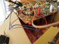
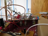
-Take a single-sided copper-clad board, drill holes in it for the valve holders and mount the valve circuits and the 74AHCT74 flip-flops on it. Use the copper as a -300 V plane. Make sure the 74AHCT74s are close to the -300 V plane, but well isolated from it. Also make sure you don't accidentally short the -300 V to ground, especially not through your body.
See the attached photos. For mounting the 74AHCT74 ICs (among other things), I had some very small single-sided PCBs that I could glue to the -300 V plane and then solder ICs in DIL package on.
-Use perfboard without copper islands for the power supply (as seen in the foreground of the second photo)
-Use a Trenz carrier board for the FPGA module, see https://shop.trenz-electronic.de/en...ard-with-unsoldered-headers-for-TE0300/TE0630. This will require some changes in the user constraint file of the FPGA code because some of the outputs I use are not on the headers of the carrier board, but I can help you with that.
-Use adapter boards and perfboard for the SRC4392 and DIX4192, such as QFP48-56 / LQFP48-56 / TQFP48-56 SMD Adapter Board (0.5mm and 0.65mm pitch), embedded-channel.de
For the reconstruction filter you could use the single-ended variant and maybe use potcores that are one size smaller than the ones I used. I chose rather large ones to be absolutely sure they wouldn't dominate the distortion, but with one size smaller they still shouldn't dominate.
Attachments
Last edited:
I would want to stick with a 4-layer PCB and SMD but experiment with the mounting of the valves. It needs to be of a certain size in order to stack with something else.
By the way, I estimate that the size of the main PCB can be reduced to about 250 mm by 280 mm when all the not so critical circuitry is removed from it, some axial parts are replaced with radial ones and the digital circuitry is shifted up a bit. This would reduce the Eurocircuits price to
euro 281.02 for 1 PCB
euro 225.96 per PCB when you order 2 of them
euro 179.84 per PCB when you order 3 of them
euro 281.02 for 1 PCB
euro 225.96 per PCB when you order 2 of them
euro 179.84 per PCB when you order 3 of them
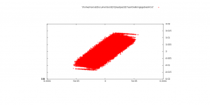
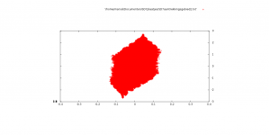
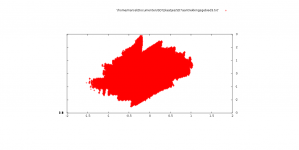
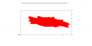
Just out of curiosity I've plotted some intersections of the basin of attraction of the seventh-order chaotic sigma-delta (with clippers switched off). Its basin of attraction is a seven-dimensional figure defined by all combinations of integrator start values that do not result in instability.
These plots have no practical use as far as I know, but I knew from Lars Risbo's PhD thesis that they can be very pretty. My plots are not nearly as pretty as Risbo's, though.
These plots have no practical use as far as I know, but I knew from Lars Risbo's PhD thesis that they can be very pretty. My plots are not nearly as pretty as Risbo's, though.
Attachments
- Home
- Source & Line
- Digital Line Level
- Valve DAC from Linear Audio volume 13