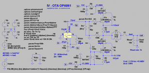
Sorry for the late response. For lpf i just use a 400pf cap parallel to the 3k9 resistor connected to pin 5 of AD844. I did a vertical stack of the opamps . 3 pieces on top of each other and soldered all the pins except for pin 1 and pin8How do you stack 3 AD844?
Hi,
comparing the AD844 with the OPA86x the +Input equals B(ase), the -Input equals E(mitter) and the TZ-Output equals the C(ollector).
One difference is the Iq-Input of the OPAs with which You can set its bias currents and control the transconductance.
Keeping an eye on the heat power losses, set Iq high.
It increases linearity and decreases the Input impedance.
A low Input impedance is important for lowest THD.
The AD soares at relatively high 50Ohms, while the OPAs settle around 10Ohms, beating even a stacked triple or quad of ADs.
Another important difference are the lower supply rails of +-5V.
That limits the maximum Output voltage to ~2.5Vrms .... but certainly enough to fully drive any power amp.
Fortunately One doesn't need any headroom like in analog systems.
The DAC outputs are limited to +1mA or -1mA maximum current ... no overhead ... hence a equally clear defined upper Output voltage limit of Idac*Riv Volts.
The therefore possible lower supply rails allow to increase the bias currents of the OPAs without the heat power losses becoming too high.
That's the reason why a single OPA can replace a pair, maybe even a triple of AD844s ... and input impedance wise even 5 to 6 of them.
I'm a bit surprised that the AD844 gets so much more attention than the OPAs, as the OPAs are not only the superior parts for this application, but offering more flexibility and even cost alot less.
jauu
Calvin
Last edited:
Keeping an eye on the heat power losses, set Iq high.
It increases linearity and decreases the Input impedance.
setting Iq high means connecting Iq directly to V- or through 50ohm resistor to the V-, correct?
Hi,
if You want to supply from +-5V a diamond Buffer made from bipolars would be ok, but probabaley not better than the Buffer integral to the OPA860.
If You ´re free regarding the supply rails a discrete Buffer can be the alternative.
Cood look like this ;-)
Its a cascoded JFET-Buffer where the ´lower part´ forms a modulated current source.
It can drive load resistances from 1k on and is virtually THD-transparent for loads >10k.
Another fine Buffer for higher load impedances would be Keantoken´s.
If You need more muscle the Calvin-Buffer -basically a beefed-up Version of the cascoded JFET-Buffer above, could drive loads down to a couple of dozens Ohm.
But for the first shots I´d recommend to use the OPA860´s internal buffer as it requires the least effort and it will for sure be no bad solution either.")
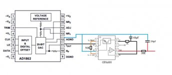
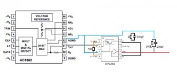
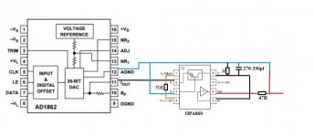
Regarding the attached I-V Converter schematic.
- C1 slightly limits the DAC´s current ´slewrate´ - optional
- Riv converts the DAC-signal current into a Voltage after: IxRiv
- Civ limits the bandwidth and provides for a clean pulse wo. overshoot (C min:68pF). I typically design Civ such that it sets the bandwidth limit to between 100-200kHz. For example: 3k3 and 270p ==> 188kHz
- Rbias is chosen 100R here, giving a bias of ~5.5mA (around 6.2mA after DS).
That should guarantee that the OPA861´s internal current mirrors run on more than 1mA idle current ... hence no paralleling of OPAs required.
In case of a too high output offset either the buffer may be trimmed or a dedicated output coupling cap may be used.
jauu
Calvin
if You want to supply from +-5V a diamond Buffer made from bipolars would be ok, but probabaley not better than the Buffer integral to the OPA860.
If You ´re free regarding the supply rails a discrete Buffer can be the alternative.
Cood look like this ;-)
Its a cascoded JFET-Buffer where the ´lower part´ forms a modulated current source.
It can drive load resistances from 1k on and is virtually THD-transparent for loads >10k.
Another fine Buffer for higher load impedances would be Keantoken´s.
If You need more muscle the Calvin-Buffer -basically a beefed-up Version of the cascoded JFET-Buffer above, could drive loads down to a couple of dozens Ohm.
But for the first shots I´d recommend to use the OPA860´s internal buffer as it requires the least effort and it will for sure be no bad solution either.
Regarding the attached I-V Converter schematic.
- C1 slightly limits the DAC´s current ´slewrate´ - optional
- Riv converts the DAC-signal current into a Voltage after: IxRiv
- Civ limits the bandwidth and provides for a clean pulse wo. overshoot (C min:68pF). I typically design Civ such that it sets the bandwidth limit to between 100-200kHz. For example: 3k3 and 270p ==> 188kHz
- Rbias is chosen 100R here, giving a bias of ~5.5mA (around 6.2mA after DS).
That should guarantee that the OPA861´s internal current mirrors run on more than 1mA idle current ... hence no paralleling of OPAs required.
In case of a too high output offset either the buffer may be trimmed or a dedicated output coupling cap may be used.
jauu
Calvin
Attachments
Last edited:
But for the first shots I´d recommend to use the OPA860´s internal buffer as it requires the least effort and it will for sure be no bad solution either.
Thank you Calvin for the detailed explanation and the schematics.
In case I'll use an OPA860 with it's buffer will the attached (very basic) circuit work?
Attachments
Hi,
no, the 3k should go from C to gnd .... parallel to the 68pF (see Riv||Civ in my schematic two posts earlier)
C also connects to the In-pin of the buffer.
Increase the 68pF to 270-330pF to reduce the bandwidth to practical values.
You may also reduce the 100R to 47R, though it doesn't make much dfference as long as the attached load is greater than a few kOhms.
Omit with the 200pF.
And don't forget to properly decouple the plus and minus supply pins with caps .
jauu
Calvin
Okay, I'll do that (-;
Thanks a lot.
BTW I'm going to use separate power supply to the AD1862 and the OPA860, which one should have the better power supply noise wise?
which power supply should be the better one for the AD1862, the digital PS or the analog PS?
Thanks a lot.
BTW I'm going to use separate power supply to the AD1862 and the OPA860, which one should have the better power supply noise wise?
which power supply should be the better one for the AD1862, the digital PS or the analog PS?
Last edited:
Hi,
@bguy
Which PS should be better ..... better in what regard?
I´m sorry but I don´t think that there´s a short one-fits-all answer to this.
It depends on the circumstances and what You want to achieve.
For sure a decent supply doesn´t require tons of Caps.
I prefer to use switching supplies follwed by a good regulator stage.
See for example Jan.Didden´s silent switcher.
@samoloko
I didn´t compare the AD to the OPAs, but generally I´d prefer a single device over stacked devices ... looking like some lowclass handicraft work.
Technically spoken, it must be insured that if the signal current exceeds the idle currents, that the stacked devices share it evenly.
Similar to paralleling output trasistors in a power amp it might otherwise happen, that one device is overdriven.
I don´t think that this is a specific problem with the ADs, but why try if I can have a ´safe´ and improved alternative for even less money?
In our DACs we sample to 176.4kHz or 192kHz and that´s about the bandwidth limit I choose for the LPF.
High enough for a good step response and low phaseshift within the audio band, yet low enough to safely keep RF outside.
If the DAC clocks at lower frequencies I´d choose a lower bandwidth limit accordingly.
I do of course look at the amplitude response of the digital filter also.
Modern filters attenuate around -100dB or more ..... which renders a analog post filter rather obsolete at all.
Even a simple RC-6dB-LP suffices ..... as it may not needed to filter out aliasing artefacts or glitches but rather to keep RF interference from entering the following stages.
Depending on what the DAC puts out even a 500kHz or higher LP-filter may then be fully ok.
With older filters/DACs the HF-attenuation may be as low as -60dB.
So there might be some artefacts left that may require a -12dB or -18dB/oct 50kHz-LP.
You may want to read this: Application Report SLEA048–May 2005 "Out-of-Band Noise and Filtering for PCM DAC" from the TI website
and
Application Report SLAA313–December 2006 "Out-of-Band Noise Measurement Issues for Audio Codecs" also from TI
jauu
Calvin
Dear Calvin, I know it's an old thread, unfortunately I didn't have the chance to try your suggestion yet.
What output voltage should I expect to get in the output of the OPA860 using the attached scheme?
3k * 2ma = 6Vpp ~= 2.1Vrms
Hi,
it will be 0V, as the output of the buffer stage is shorted to agnd
If You cut the red/blue link behind the 47R the output voltage will be the AD's output current times 3000, a small output offset voltage not accounted for.
IIrc the AD puts out up to +-1mA, which then gives +-3000mV peak-peak, or ~2.1Vrms (rem: depending on the load impedance the buffer output sees. The DS specs a factor of 0.98 for a load of 500R)
The 50R Iq-setting resistor I'd choose either 47R (same as the output resistor, for lower different parts number count) or 250r as TI suggests in the datasheet and which is sufficiently high for +-1mA current swing to keep the internal stages biased in class A.
It reduces the overall Iq ... not by much.... but anyway it reduces heat power losses a bit.
jauu
Calvin
Hi,
it will be 0V, as the output of the buffer stage is shorted to agnd
If You cut the red/blue link behind the 47R the output voltage will be the AD's output current times 3000, a small output offset voltage not accounted for.
Yes, of course, there was something in between and I forgot to erase the trace of it.
Do you think it would be better to use the 250R as TI suggested?
Hi,

If You look at Fig.12 of the DS (and compare with Fig.11 of the OPA861 DS, the Buffer-less Brother) one can estimate that the difference in Iq between 50R and 250R are only 1.2-1.4mA (12.6mA vers. 11.4mA, 6.8mA vers. 5.4mA for the OPA861).
The nearly same change in Bias current gives a hint, that the Buffer´s Bias remains almost constant, indicating that only the Bias current of the I/V part changes.
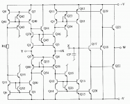
Now, if one looks at the schematic of the almost identical AD844 (attachment) we see that the Buffer consists of Q17 to Q20 and that there are four ´legs´ between which Iq divides.
For the AD844 the leg Q6-RQ-Q8 is biased at 150µA (fixed value, Rq= internal resistor).
And we can safely assume that the legs Q5-Q7, Q14-Q11 and Q15-Q12 run on the same Bias current value.
Those are the legs hat also carry/convey the DAC signal current.
Their Bias current must be greater than the peak signal current (>1mA in case of a AD1862 DAC).
The OPA861´s DS shows the ratios between Rset and Iadj (Fig.17) and Iq/Iadj (Fig.16).
So we can calculate the Bias in the remaining three legs of the OPA861 resp. we can estimate the Bias current of the OPA860´s legs also.
Its (Iq-Iadj)/3.
For the OPA860 and AD844 its (Iq-Ibuffer-Iadj)/3 .... unfortunately Ibuffer of the AD844 remains uncertain.
The OPA861´s Buffer oviously runs on 5.8mA-6mA.
Taking the afore mentioned 5.8-6.8mA of Iq of the OPA861 int account, then the Bias of the three legs varies between 1.8mA and 2.27mA.
From Fig.21 (Fig.16 of OPA860) the OTA Transfer Characteristic show a inceasing linearity with rising Bias.
Though we don´t use the OPAs as OTAs in its basic meaning here, there´s a small input voltage due to the non-0 input impedance of <+-20mV.
Over that range the Bias variation between 50R and 250R is almost negligable.
It probabely has only a effect on heat power loss.
With 250R the OPA runs a bit cooler .... that´s probabely all.
But maybe if the R is increased vastly, Bias could come down far enough that the Linearity reduces so much (distortion rises) that it may even become audible.
Something for show and tell.
jauu
Calvin
Well, I don´t knowDo you think it would be better to use the 250R as TI suggested?
If You look at Fig.12 of the DS (and compare with Fig.11 of the OPA861 DS, the Buffer-less Brother) one can estimate that the difference in Iq between 50R and 250R are only 1.2-1.4mA (12.6mA vers. 11.4mA, 6.8mA vers. 5.4mA for the OPA861).
The nearly same change in Bias current gives a hint, that the Buffer´s Bias remains almost constant, indicating that only the Bias current of the I/V part changes.
Now, if one looks at the schematic of the almost identical AD844 (attachment) we see that the Buffer consists of Q17 to Q20 and that there are four ´legs´ between which Iq divides.
For the AD844 the leg Q6-RQ-Q8 is biased at 150µA (fixed value, Rq= internal resistor).
And we can safely assume that the legs Q5-Q7, Q14-Q11 and Q15-Q12 run on the same Bias current value.
Those are the legs hat also carry/convey the DAC signal current.
Their Bias current must be greater than the peak signal current (>1mA in case of a AD1862 DAC).
The OPA861´s DS shows the ratios between Rset and Iadj (Fig.17) and Iq/Iadj (Fig.16).
So we can calculate the Bias in the remaining three legs of the OPA861 resp. we can estimate the Bias current of the OPA860´s legs also.
Its (Iq-Iadj)/3.
For the OPA860 and AD844 its (Iq-Ibuffer-Iadj)/3 .... unfortunately Ibuffer of the AD844 remains uncertain.
The OPA861´s Buffer oviously runs on 5.8mA-6mA.
Taking the afore mentioned 5.8-6.8mA of Iq of the OPA861 int account, then the Bias of the three legs varies between 1.8mA and 2.27mA.
From Fig.21 (Fig.16 of OPA860) the OTA Transfer Characteristic show a inceasing linearity with rising Bias.
Though we don´t use the OPAs as OTAs in its basic meaning here, there´s a small input voltage due to the non-0 input impedance of <+-20mV.
Over that range the Bias variation between 50R and 250R is almost negligable.
It probabely has only a effect on heat power loss.
With 250R the OPA runs a bit cooler .... that´s probabely all.
But maybe if the R is increased vastly, Bias could come down far enough that the Linearity reduces so much (distortion rises) that it may even become audible.
Something for show and tell.
jauu
Calvin
Attachments
- Home
- Source & Line
- Digital Line Level
- I/V and analog output stage for AD1862