Assembling the PCB
Sorry Guys for the delay.. Was very busy this week
ASSEMBLE:
To assemble the board there is not much to say.
Make sure that you work on a clean surface..
May a PCB holder would be fine for the one or other, as there it is possible to access both sided and have both hands free for working.
Make sure the the Copper of the PCB is clean without grease *ex. from your fingers* dust or other things..
Prior to assemble you had to drill, so make sure that all holes have been drilled.. * self check drilling*
Start with the small components first and pull the wires thru the board, Check that the VALUES of the Components facing in the same direction from left to right and from up to down.. so, if ones this PCB has to be repaired one does not need to turn the board 50 times because the components are assembled chaotic..
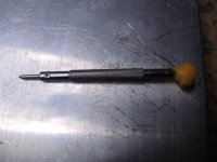
Use a Solder iron with low heat but HOT.! 20 watts is more than enough for Resistors, Capacitors, Diodes, and also Transistors, no need to have an iron with 100 watts and more..
I use a dual wattage Soldering Iron, with push on a small switch I can boost it up tp 200Watts, for real thick things..
try to wear this silicone gloves while assembling this helps to keep fingerprints off the board. this are the most important things..
Use a good Side Plier Cutting tool to cut the leftover legs from transistors and Resistor as close as possible to the soldering joint.. This makes it looks nice and professional, no need to bend the Wires of the Components too much 75 degree angel is good enough
Id you have to solder wires ie. Signal wires to the PCB use Shrink rubber to close up the finish before the wire hit the PCB.. If you pull isolation thru the PCB then make a small slope so the wire will be stress free while installing the PCB into the BOX..
If you place connectors then make sure that on can access the plugs sticking in the connectors, easy..
May anyone else have some more knowledge..
thanks for reading..
Chris Hess
Sorry Guys for the delay.. Was very busy this week
ASSEMBLE:
To assemble the board there is not much to say.
Make sure that you work on a clean surface..
May a PCB holder would be fine for the one or other, as there it is possible to access both sided and have both hands free for working.
Make sure the the Copper of the PCB is clean without grease *ex. from your fingers* dust or other things..
Prior to assemble you had to drill, so make sure that all holes have been drilled.. * self check drilling*
Start with the small components first and pull the wires thru the board, Check that the VALUES of the Components facing in the same direction from left to right and from up to down.. so, if ones this PCB has to be repaired one does not need to turn the board 50 times because the components are assembled chaotic..
Use a Solder iron with low heat but HOT.! 20 watts is more than enough for Resistors, Capacitors, Diodes, and also Transistors, no need to have an iron with 100 watts and more..
I use a dual wattage Soldering Iron, with push on a small switch I can boost it up tp 200Watts, for real thick things..
try to wear this silicone gloves while assembling this helps to keep fingerprints off the board. this are the most important things..
Use a good Side Plier Cutting tool to cut the leftover legs from transistors and Resistor as close as possible to the soldering joint.. This makes it looks nice and professional, no need to bend the Wires of the Components too much 75 degree angel is good enough
Id you have to solder wires ie. Signal wires to the PCB use Shrink rubber to close up the finish before the wire hit the PCB.. If you pull isolation thru the PCB then make a small slope so the wire will be stress free while installing the PCB into the BOX..
If you place connectors then make sure that on can access the plugs sticking in the connectors, easy..
May anyone else have some more knowledge..
thanks for reading..
Chris Hess
very inspiring thread!
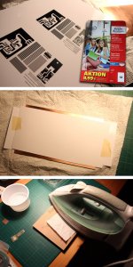
i prefer to do the direct (heat) toner transfer method, which for me was faster and more accurate.
i got inspiration from mr carlson's lab:
Make A Circuit Board, At Home! - YouTube
after some unsuccessful tests with glossy catalogue paper i tried one-sided high gloss inkjet paper as suggested in the video and it works great.
i slide both paper sheets to fit exactly checking the overlapping of small holes, using a normal desk lamp and secure the sheets with adhesive tape (stay outside the PCB area, for better ironing results).
i make sure to clean both copper surfaces and deburr all edges, then slide the clean PCB material between the paper sheets.
using a hot flat iron i transfer the toner from paper to copper. i use a paper towel between iron and paper and a flat MDF board, that keeps the heat where it should be. the iron is on it's hottest setting and i press it thoroughly on the PCB, trying to reach all surfaces. same ironing procedure on the other side. the more pressure, heat and time the better! but do not press and move too hard at the same time, as it might smear the toner.
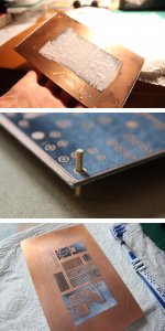
i let the PCB cool down and then wash and rub away the paper with warm water, soap and an old tooth brush. once the board and the toner is dry i check for paper coating that usually remains on the PCB and either scratch it away with a sharp knife (dangerous) or once more use soap and tooth brush (better).
the toner sticks very well on the copper, however it is easily scratched. if this happens i correct it with permanent marker.
next step: etching (i use iron-III-chloride). small pieces of tooth pick at the mounting holes help for the etching process.
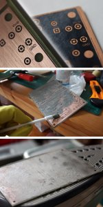
as can be seen on the photos this method tends to make traces thinner than drawn and printed. i now use wider minimum trace width for thermal pads.
i also tried to tin-coat the etched PDB using "water-fitting" soldering paste. it does work, using the flat iron upside down and then washing away the residue of this process with water. not sure how efficient the coating and how harmful the soldering paste is, however.
inspired by user lmao i used glass and porcelain paint ("kreul") to make a decorative, protective and isolating "solder mask" (it does not really withstand the heat of the soldering iron for long...).
i got the best results by tinning the solder points with the soldering iron (for a shiny and non-sticky surface) and covering them with masking gum. after drying of the masking gum i paint the PCB with a DIY airbrush, using thinner for the glass-paint.
after the paint has dried i cure it in the oven at 170°C.
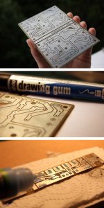
only after this the masking gum (and cured paint) is easily removed from the solder points. next step: drilling and finally assembling.
as you can see on the last photo a SMD-PCB for a TPA3116 is probably the dimension limit of this method... i will try it anyway!
i prefer to do the direct (heat) toner transfer method, which for me was faster and more accurate.
i got inspiration from mr carlson's lab:
Make A Circuit Board, At Home! - YouTube
after some unsuccessful tests with glossy catalogue paper i tried one-sided high gloss inkjet paper as suggested in the video and it works great.
i slide both paper sheets to fit exactly checking the overlapping of small holes, using a normal desk lamp and secure the sheets with adhesive tape (stay outside the PCB area, for better ironing results).
i make sure to clean both copper surfaces and deburr all edges, then slide the clean PCB material between the paper sheets.
using a hot flat iron i transfer the toner from paper to copper. i use a paper towel between iron and paper and a flat MDF board, that keeps the heat where it should be. the iron is on it's hottest setting and i press it thoroughly on the PCB, trying to reach all surfaces. same ironing procedure on the other side. the more pressure, heat and time the better! but do not press and move too hard at the same time, as it might smear the toner.
i let the PCB cool down and then wash and rub away the paper with warm water, soap and an old tooth brush. once the board and the toner is dry i check for paper coating that usually remains on the PCB and either scratch it away with a sharp knife (dangerous) or once more use soap and tooth brush (better).
the toner sticks very well on the copper, however it is easily scratched. if this happens i correct it with permanent marker.
next step: etching (i use iron-III-chloride). small pieces of tooth pick at the mounting holes help for the etching process.
as can be seen on the photos this method tends to make traces thinner than drawn and printed. i now use wider minimum trace width for thermal pads.
i also tried to tin-coat the etched PDB using "water-fitting" soldering paste. it does work, using the flat iron upside down and then washing away the residue of this process with water. not sure how efficient the coating and how harmful the soldering paste is, however.
inspired by user lmao i used glass and porcelain paint ("kreul") to make a decorative, protective and isolating "solder mask" (it does not really withstand the heat of the soldering iron for long...).
i got the best results by tinning the solder points with the soldering iron (for a shiny and non-sticky surface) and covering them with masking gum. after drying of the masking gum i paint the PCB with a DIY airbrush, using thinner for the glass-paint.
after the paint has dried i cure it in the oven at 170°C.
only after this the masking gum (and cured paint) is easily removed from the solder points. next step: drilling and finally assembling.
as you can see on the last photo a SMD-PCB for a TPA3116 is probably the dimension limit of this method... i will try it anyway!
Attachments
Last edited:

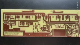
Hi Gents,
You might wonder why everything is quiet,,,
Lots of work and Final PCB VERSION will be made tomorrow..
Downsized the PCB to 100 mm x 296mm instead of 110 and 300..
Reason, nothing special but just to have less leftovers, with not usable sizes..
So, check back tomorrow..
Regards
Chris
You might wonder why everything is quiet,,,
Lots of work and Final PCB VERSION will be made tomorrow..
Downsized the PCB to 100 mm x 296mm instead of 110 and 300..
Reason, nothing special but just to have less leftovers, with not usable sizes..
So, check back tomorrow..
Regards
Chris
Attachments
Last edited:
"Final" PCB?
Sunday again,
Hi Gentlemen
OK After getting some Customers PC back to life, I had some spare time, it's almost 3pm on a Sunday, to get this layout onto a PCB.. Size as I mentioned 100mm X 296 mm the tracks board is 100mmX300mm
It's done and I think this will be the final one.. If I do not find some bad or missing Tracks.. Somehow I got some Dirt in the Etching solution, which gave me a bad spot on the PCB.. but never mind, a few stripes with the ART KNIFE, and the problem has been solved,,
After Protection Fluid has been applied, it will not show anymore.. so no harm done. Got new Drilling machines yesterday, with laser Guide and especially to make PCB's. So drilling holes for the rest of the time coming..
Enjoy weekend Guys..
Have a nice Sunday..
Attachments
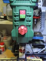
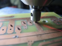
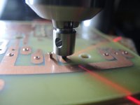
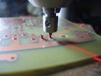
Got new Drilling machines yesterday, with laser Guide and especially to make PCB's.
Now that is something you must show us
")
Nothing special all newer drill using this system
It's nothing special, the "laser Guide" as they call is only to point the Drill exactly to the center of the hole which has been drilled. It uses two *I think LED's* which make a cross hair in which matches the center of the drill.
The same system I have on that PCB Cutter I use.
Holes less than 1mm I drill by hand, with the PCB stand, it's much faster, than moving the PCB and center this with the Cross hair. Usually I do not miss the center of the holes..
It's none Step Variable Speed, and was real inexpensive, otherwise I wouldn't buy it.. As I have already a big Size Table Stand Drill. Now I have two..
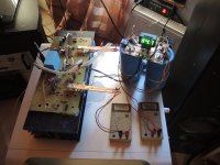
this board, I have checked and right now assemble it.
Plugged in the prototype of this one, which is on my working table, which I did not switch on for almost a month..
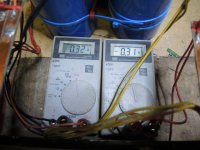
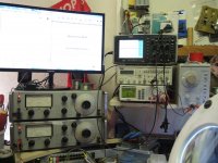
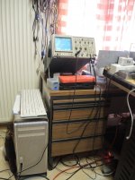
So hooked up 4Ohm speakers and listened to it.. And It's just a dream how it sounds. And again, It's Class A Idle Current is 380milli Ampere. @+ -42Volts Rail voltages ... Filtering Caps are 68'000uf x2 Single Bridge 400Volts 25Amps. No noise no Hum, output Voltage @4 Ohms is 16Volts RMS, with less than 0.1%distortion over the full bandwidth. How much this is you will see soon. Updated my Table and also instruments I use, to measure, New Curved 24" Flat Screen for the MAC PRO, with REW installed on Windows Server 10. Now I can measure in the same Time Distortion on both channels with the HP Distortion analyzers, and also check all on the computer hooked to the sound card with a TASCAM interface. as well as have the the curves displayed on the Le Croy 100Mhz Oscilloscope.
Specs will follow soon again in a video and as Pics as well. Think the amp will be ready Sunday.
Also got some through the hole improvements for the Rail and GND connectors. All my Amps have Power Clamps screwed to the PCB instead of soldered. Now this Clamps I make by hand and testing them. Cables are not soldered to the clamps and also not Pressed with a grip.. But are hold with a "conical wire clamp" screwed into the Clamp with will be screwed onto the board. all made out of Copper and gold Plated. this one, I'm testing right now,. got only three of them as it's a lot of work to do these, takes more than 2 hours per piece.. That way I might here some difference of the sound, because Solder is missing from the rails, I'm interested to hear how it sounds, when only copper to copper transfers the Voltages and Amperes which it takes to feed that amp..
And for the Greenies, the Amp takes 60Watts Idle.. * I was hoping that it would be less, but it's not final yet, this is only the Prototype which I tested again tonight* not bad for a Class A which can deliver up to 100Watts RMS into 2 Ohms. But of course then it takes about 5 AMPs per Channel... But no one is listening on full load @2 Ohms all the time..
So we could say it's a green Class A, and the ICE BEAR in the Arctic don't need to worry that because of my amp, the ice would melt away.
So that are the news..
Pictures will follow. Not now thou, it's midnight here in Swiss... and I ought to go to sleep, have to get up at 6:30
Greetings
Chris
It's nothing special, the "laser Guide" as they call is only to point the Drill exactly to the center of the hole which has been drilled. It uses two *I think LED's* which make a cross hair in which matches the center of the drill.
The same system I have on that PCB Cutter I use.
Holes less than 1mm I drill by hand, with the PCB stand, it's much faster, than moving the PCB and center this with the Cross hair. Usually I do not miss the center of the holes..
It's none Step Variable Speed, and was real inexpensive, otherwise I wouldn't buy it.. As I have already a big Size Table Stand Drill. Now I have two..
this board, I have checked and right now assemble it.
Plugged in the prototype of this one, which is on my working table, which I did not switch on for almost a month..
So hooked up 4Ohm speakers and listened to it.. And It's just a dream how it sounds. And again, It's Class A Idle Current is 380milli Ampere. @+ -42Volts Rail voltages ... Filtering Caps are 68'000uf x2 Single Bridge 400Volts 25Amps. No noise no Hum, output Voltage @4 Ohms is 16Volts RMS, with less than 0.1%distortion over the full bandwidth. How much this is you will see soon. Updated my Table and also instruments I use, to measure, New Curved 24" Flat Screen for the MAC PRO, with REW installed on Windows Server 10. Now I can measure in the same Time Distortion on both channels with the HP Distortion analyzers, and also check all on the computer hooked to the sound card with a TASCAM interface. as well as have the the curves displayed on the Le Croy 100Mhz Oscilloscope.
Specs will follow soon again in a video and as Pics as well. Think the amp will be ready Sunday.
Also got some through the hole improvements for the Rail and GND connectors. All my Amps have Power Clamps screwed to the PCB instead of soldered. Now this Clamps I make by hand and testing them. Cables are not soldered to the clamps and also not Pressed with a grip.. But are hold with a "conical wire clamp" screwed into the Clamp with will be screwed onto the board. all made out of Copper and gold Plated. this one, I'm testing right now,. got only three of them as it's a lot of work to do these, takes more than 2 hours per piece.. That way I might here some difference of the sound, because Solder is missing from the rails, I'm interested to hear how it sounds, when only copper to copper transfers the Voltages and Amperes which it takes to feed that amp..
And for the Greenies, the Amp takes 60Watts Idle.. * I was hoping that it would be less, but it's not final yet, this is only the Prototype which I tested again tonight* not bad for a Class A which can deliver up to 100Watts RMS into 2 Ohms. But of course then it takes about 5 AMPs per Channel... But no one is listening on full load @2 Ohms all the time..
So we could say it's a green Class A, and the ICE BEAR in the Arctic don't need to worry that because of my amp, the ice would melt away.
So that are the news..
Pictures will follow. Not now thou, it's midnight here in Swiss... and I ought to go to sleep, have to get up at 6:30
Greetings
Chris
Last edited:
Laser for drill:
Here's one, though I suspect it could be better.
https://www.amazon.com/Wixey-Model-WL133-Drill-Press/dp/B01NAT54TX

Here's one, though I suspect it could be better.
https://www.amazon.com/Wixey-Model-WL133-Drill-Press/dp/B01NAT54TX
Attachments
CongratulationsPlugged in the prototype of this one, which is on my working table, which I did not switch on for almost a month..
So hooked up 4Ohm speakers and listened to it.. And It's just a dream how it sounds.
Here a few Pics
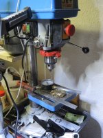
Guys
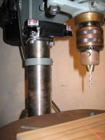
Here as promised the Pics of that Drill. The Drill cost a 100Bucks.. that's why I bought it.. To be exactly it was 99Bucks. Till now I'm satisfied. It has also a part holder as we can see which frees the Hand of the operator to do other things instead of holding the Piece which has to be drilled.
The through-hole connection I made that way to make sure my Cables, (6sqmm) have real good connection with GND. Screw will fit in there just fine and can be fastened without and Extra Nut on opposite Site.
For this Board (which will be my last) it's only used for the GND terminal..
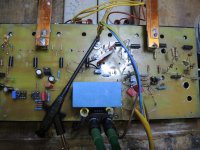
Also a few Pics of the Prototype.. with Current consumption & Voltage board layout.. this is board number 2.. the one you see in the last post is number 5..
Number 1. Not build because of bad Quality
Number 2. This one in this pic
Number 3 & 4 Not build because I did not like it..
Number 5 = the final one I hope, this is the one with that Through hole connector..
Forgive me the mess on the table. I'm working on it.. as soon the table is clean you will get a shot of the full working Table..
Luckily I will stop to produce amps, after this one and the Line drive, otherwise I would need to extend the Table. because of not enough space..
Guys
Regards Chris
Guys
Here as promised the Pics of that Drill. The Drill cost a 100Bucks.. that's why I bought it.. To be exactly it was 99Bucks. Till now I'm satisfied. It has also a part holder as we can see which frees the Hand of the operator to do other things instead of holding the Piece which has to be drilled.
The through-hole connection I made that way to make sure my Cables, (6sqmm) have real good connection with GND. Screw will fit in there just fine and can be fastened without and Extra Nut on opposite Site.
For this Board (which will be my last) it's only used for the GND terminal..
Also a few Pics of the Prototype.. with Current consumption & Voltage board layout.. this is board number 2.. the one you see in the last post is number 5..
Number 1. Not build because of bad Quality
Number 2. This one in this pic
Number 3 & 4 Not build because I did not like it..
Number 5 = the final one I hope, this is the one with that Through hole connector..
Forgive me the mess on the table. I'm working on it.. as soon the table is clean you will get a shot of the full working Table..
Luckily I will stop to produce amps, after this one and the Line drive, otherwise I would need to extend the Table. because of not enough space..
Guys
Regards Chris
Attachments
-
 9Prototype Board on Heatsink.jpg227.3 KB · Views: 60
 -
 8.1 Idle Current Protitype.jpg173.4 KB · Views: 64
 -
 8. Prototype.jpg208.4 KB · Views: 60
 -
 7. Prototype Idle@300milliampere.jpg251.7 KB · Views: 66
 -
 6.Through Hole Connection.jpg139.5 KB · Views: 60
 -
 5. Drill Setup.jpg296.1 KB · Views: 61
 -
 4. Attention Laser.jpg237.6 KB · Views: 55
 -
 3. Laser Pointening System.jpg252.5 KB · Views: 59
 -
 2. Old Drill Mashine.jpg349.5 KB · Views: 72
 -
 1. Parkside Dfill.jpg256.2 KB · Views: 77
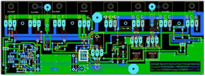
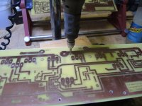
Board Version 10.00.60 has been done, hopefully it's the last one.
Hi everyone
After a month of Burning AMP Switzerland where it almost drove me nuts, not finding a valuable Working Point for that Variable Current Source Class A Amp and burned about 25 Drive Transistors, finally, changing Rail Voltages helped to cure most of the problems./ but this don't mean that I will not try to get that 42 +- voltages Rail to work.. Working on it.
Now, the Boards I showed in my last post, had to be redesigned again, slightly so, it is possible to use different Rail Voltages, also different Transistors, without loosing to much sound Quality..
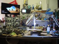
Here you can see the newly made Boards *yesterday*, and drilled them today,
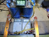
also you can see my Workbench, as it really is *cleaned up the usual mess* then also the sound source with the Turntable and the Mixing Console which is a Fostex Studion 12 channel Mixer and also the First or Prototype of that Variable Current Source Amp. running on only 0.36 - 0.38 milliampere while Idle or under 3 Watts on a 4 Ohm load.
Never thought that a Class A can sound good running only on about 0.4Amps Idle but this one sounds real good.. Had it running for 10 hours and more continued and heat was something like 35degrees Celsius..
The amp will heat up when driven into high output power levels but no FANS ARE needed.
BTW the Prototype runs on 4 output Transistors only, the new board will run on all transistors it was designed for 8 to be exactly.
No excessive heat, while on Idle - now stable already for two weeks comparing it to the Single End which pulls 700Watts Idle.. this one pulls only around 35 Watts Idle / Measured.
Will start to build it in the coming days, as time allows..
For everyone who had the fortune to attended BAF 2021, I'm turning jealous, and hope you guys had fun.. to see the Masters of Amplifier techniques in real....
Leave you with a few Pics from today..
Regards
Chris Hess
Hi everyone
After a month of Burning AMP Switzerland where it almost drove me nuts, not finding a valuable Working Point for that Variable Current Source Class A Amp and burned about 25 Drive Transistors, finally, changing Rail Voltages helped to cure most of the problems./ but this don't mean that I will not try to get that 42 +- voltages Rail to work.. Working on it.
Now, the Boards I showed in my last post, had to be redesigned again, slightly so, it is possible to use different Rail Voltages, also different Transistors, without loosing to much sound Quality..
Here you can see the newly made Boards *yesterday*, and drilled them today,
also you can see my Workbench, as it really is *cleaned up the usual mess* then also the sound source with the Turntable and the Mixing Console which is a Fostex Studion 12 channel Mixer and also the First or Prototype of that Variable Current Source Amp. running on only 0.36 - 0.38 milliampere while Idle or under 3 Watts on a 4 Ohm load.
Never thought that a Class A can sound good running only on about 0.4Amps Idle but this one sounds real good.. Had it running for 10 hours and more continued and heat was something like 35degrees Celsius..
The amp will heat up when driven into high output power levels but no FANS ARE needed.
BTW the Prototype runs on 4 output Transistors only, the new board will run on all transistors it was designed for 8 to be exactly.
No excessive heat, while on Idle - now stable already for two weeks comparing it to the Single End which pulls 700Watts Idle.. this one pulls only around 35 Watts Idle / Measured.
Will start to build it in the coming days, as time allows..
For everyone who had the fortune to attended BAF 2021, I'm turning jealous, and hope you guys had fun.. to see the Masters of Amplifier techniques in real....
Leave you with a few Pics from today..
Regards
Chris Hess
Attachments
-
 7. Prototype running on Plus Minus 34VoltRails.jpg175.4 KB · Views: 77
 -
 6.First Board Board Version 10.00.60 drilled Partly.jpg208.8 KB · Views: 83
 -
 5. Drilling Holes into lastest Board Version 10.00.60.jpg159 KB · Views: 121
 -
 4. REW Feed form PowerMac - Measuring Distortion.jpg217.2 KB · Views: 131
 -
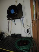 3. Sound Source & fostex Mixing Console.jpg331.4 KB · Views: 123
 -
 2. MAC Dual Xeon - W10 LTSB.jpg343.1 KB · Views: 135
 -
 1. Workbench.jpg257.1 KB · Views: 131
Last edited:
Get the board through the hole the easy way
Hi
As you see in my post from yesterday, I made now boards.
Now going a step further I thought how it would look to get this double sided boards Through hole in an other way than just soldering in wires..
So this is what I tried this morning @ 6:30 am..
I created a Stencil very small one.. and you can see that in the pictures I add here..
Using a small press will give better results than using the hammer.
The Board I used is just a board for testing out things..
Now I will give that to be made as a tool. hopefully inexpensive..
it's just an approach to get more out of the board..
Sorry Pictures aren't as sharp as these should be.. I will take care of this later again as soon I get home.
and of course DIY
Check out the pictures..
Regards
Chris Hess
Attachments
-
 6. Bottom Side Layer mid size.jpg88.8 KB · Views: 65
 -
 5. Top side Layer middle side.jpg78.5 KB · Views: 63
 -
 4. Bottom Side Layer.jpg79.5 KB · Views: 66
 -
 3. top side Layer.jpg69.5 KB · Views: 64
 -
 2. Stencil_02.jpg111.5 KB · Views: 73
 -
 1. Stencil_01.jpg63.7 KB · Views: 81
 -
 0. loetoesen_small.jpg133.4 KB · Views: 87
 -
 2.0 Stencil.jpg56.2 KB · Views: 92
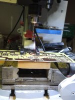
Through Hole How To or How it could be done
So Guys
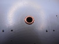
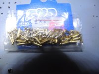
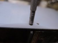
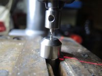
Again over a month passed, had to get the right tools and right rivets to make this Double Sided Board, through hole.
But I'm surely still not that satisfied with the outcome..
Too much waste as the Rivets differ in the diameter Size and drilling the hole larger than the outside diameter of the rivets will make then to fall out when trying to press them.
Making the hole just about right then I will waste 2 - 3 Rivets in about 10 holes.. because of crushing them..
I bought expensive pressing tools except the Press I do have this already..
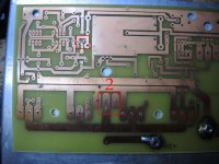
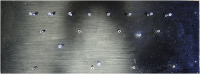
I guess I need to make the boards another time because of giving not enough space between a Transistor Screw mounting hole and a Track on top side of the board.. RED SQUARE & Number 1. looks Quite ugly
then also not clean pressed rivets on the bottom side.. RED SQUARE & Number 2
Check out the pics. BTW the tool cost 70 bucks.
1.2mm rivets @1000 Pieces 20 Bucks..
It is worth it,, when finished it will look like a dream high polished Copper Board, with a thin coat of lacquer applied..
Get back to you guys soon..
Regards Chris
So Guys
Again over a month passed, had to get the right tools and right rivets to make this Double Sided Board, through hole.
But I'm surely still not that satisfied with the outcome..
Too much waste as the Rivets differ in the diameter Size and drilling the hole larger than the outside diameter of the rivets will make then to fall out when trying to press them.
Making the hole just about right then I will waste 2 - 3 Rivets in about 10 holes.. because of crushing them..
I bought expensive pressing tools except the Press I do have this already..
I guess I need to make the boards another time because of giving not enough space between a Transistor Screw mounting hole and a Track on top side of the board.. RED SQUARE & Number 1. looks Quite ugly
then also not clean pressed rivets on the bottom side.. RED SQUARE & Number 2
Check out the pics. BTW the tool cost 70 bucks.
1.2mm rivets @1000 Pieces 20 Bucks..
It is worth it,, when finished it will look like a dream high polished Copper Board, with a thin coat of lacquer applied..
Get back to you guys soon..
Regards Chris
Attachments
-
 8. Pressed Bottom side_s.jpg896.1 KB · Views: 61
 -
 7. Pressed Top side_s.jpg655.3 KB · Views: 64
 -
 6. Pressed Bottom Side_s.jpg94.4 KB · Views: 64
 -
 5. through hole_s.jpg84.9 KB · Views: 61
 -
 4. through hole_s.JPG86.5 KB · Views: 59
 -
 3. insertion tool_s.jpg151.3 KB · Views: 55
 -
 2. Inserting tool_s.jpg184.5 KB · Views: 70
 -
 1. Rivets_s.jpg165.6 KB · Views: 72
 -
 0. Adjusting Tools_s.jpg111.2 KB · Views: 76
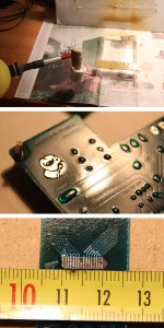
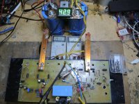
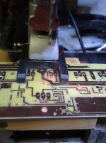
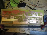
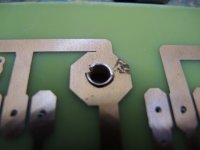
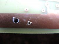
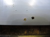
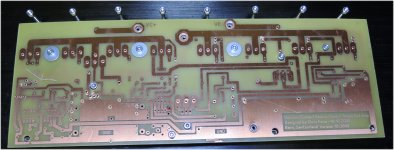
Board & Heat Sink alignment
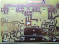
This post is prior to assemble the board, so it has to be fitted to the Heat sink that all the bolts are in place, and that the holes in the board are fitting the ones previously already drilled to the Heat Sink.
The 8 Screws at the top are for fastening the Power Transistors.
Then the 4 on the board in the upper half, are there to keep the Board in place,
Then there are 3 more which will pass through the board to fasten the Drive Transistors to the Heat Sink as well. This means that only 1 Transistor is on top of the board, as well at 2 Regulators which are regulating the PID Voltage of the these 2 On Board IC's which are guarding the VCD Output Voltage at the Speaker Terminal to make sure that there is always no Occurrence of DC.
BTW this on the left side in the right picture which is looking like a scratch, is just a piece of cloth from cleaning, no scratch on the board.. at least not in that place.
Enjoy Weekend, we are just a few hours away from that.
Chris
Attachments
Last edited:
- Home
- Design & Build
- Construction Tips
- Making a double Sided PCB Guide - how it could be done..