This here is my Bungard process.
I make my boards usually single sided + GND
That makes top & bottom alignment easy / unnecessary.
< 1__layout | Gerhard Hoffmann | Flickr >
+ the some pics to the right.
Yes, I know JLCPCB. I just got 3 different designs from then 2 weeks ago.
But my process is 2 hours from artwork in the computer to soldering.
Told you before that you make beautiful PCB's no doubt about this..
I do not like JUMPS on my Amps. And these Amp are usually drawing much current the last is 4AMPERE @idle..
The Reason I do not use JLCPCB is that>
Me> do you gold plate the PCB if there is need ?
PLCPCB > No we don't
Me> So, If I would request that connection points are gold plated this would mean that you would not make the PCB for me, right?
PLCPCB> Correct
ME > OK thank you, no deal..
There are other Manufacturers, but also the play like god in heaven, which I dislike very much, so I make my boards and then if there is need to Galvanic Gold Plating it, I have friend who works in a company who makes PCB for a Car Manufacturer, and there everything is gold plated.. no problem cost a few bucks but it is done..
About drilling
As JMFAHEY already wrote you will need to invest some money into your Tools, that the results become good and nice..
It's not only nice to have nice colors on the PCB, it's more important that you get the right size of holes for your components..
Use high-speed Dremel, 20k RPM is what it takes to get nice looking holes..
USE Carbide High Speed Drills.
Go from the smallest to the bigger drill size and take your time, no need to hurry there is nothing to win, except a beautiful board. and therefore it's better to work exactly, so you will earn respect even with your DIY BOARD..
That was it about drilling.. I drill my boards freehand in the PCB holder, because I'm used to it that way. but it is still better and more professional to take stand Drill machine like you can see in the picture Gerhard placed in his post..
I have a similar one, but I use it seldom..
After drilling make sure to get that Board Cleaned and take of these brows from drilling.. because it makes the soldering much easier, also through hole assembling is easier..
And while you at it, check for short circuits, check for broken tracks,, this can always happen. I will place a special way in one of my next posts, to make VIAS trough hole. which are looking very professional and especially for through holes where other parts are mounted on top of it..
Greetings
Chris Hess
Follow up will be interesting, it's about Assembling..
I will update the first post of this thread with links so you do not need to look for all through the post, just hit ie. Drilling and there you go..
some other factoids:
I use Zweckform/Avery film 3491 (Buy Blank & Printed Labels & Stickers Online | Avery)
"films for print mastering production". It is slightly rough, the toner attaches nicely.
When exposing the board, the toner side _must_ be towards the board.
If it needs to be really good, I go to print shop and let them make an offset film.
You cannot beat the contrast with anything else. It does not matter if your exposure
time ist 5 times too long. They take .pdf files as input and it is _really_ 2400dpi.
You can do 4/4 mil design rules on Bungard material. Price is abt. €10 per DIN/ISO A4 oversize.
Don't create the .pdf directly from within Altium Designer. That has bugs with round/oval pads.
Use Gerber output and print it from Camtastic, which is included. For my Kyocera laser printer
I must use size=104%.
IMHO, Proxxon is a notch better than Dremel. Use collets (Spannzange) to mount the drill bits,
not a chuck with 3 moving pieces (Bohrfutter). Vibration is much less. Don't use the Proxxon
for anything else but drilling. No off-axis load. The ball bearings will thank it. Even though
the diamond disk is handy for cutting PCBs. Proxxon has a circular saw for that.
Use safety glasses when drilling. A broken off carbide bit goes through your
eye like nothing.
I make everything on Eurocards, 100 * 160 mm. If there is leftover space, I fill it with
things like op-27 inverting/ noninverting, small voltage regulators, filter stages,
other standard stuff. You can hack something new together fast & easily when you have the
building blocks already in the drawer. I have collected quite a library over the time.
I/o is on 100 mil centers, so it fits prefabricated 100 mill boards. There are good ones
with a GND plane.
2 * 10 dB noninverting with ADA4898:
< Auswahl_00a1 | Low noise amplifier, 70 pV/rtHz after Art Of … | Flickr >
The GND plane is better visible here:
(Scott's preamplifier with the LED/photodiode bias)
< Gerhard Hoffmann has shared 1 photo with you! | Flickr >
When I bought the heat-resistant glass bowl for etching, I took an Eurocard with me.
I choose a bowl where the Eurocard just touches the bowl at the 4 corners and there is
2 mm space everywhere else. That makes sure that the bottom side is not scratched
during etching.
This stuff is good for chemo tin for the boards. I also have a silver solution,
but it contains a lot of cyanide.
Attachments
Last edited:
HiWell I mean I have a wiki article on this but more guides are always a good thing.
You did a fantastic Job, this just besides that it is very helpful.
Pull my hat with respect.!
Regards
Chris Hess
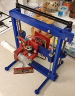
With regards to drilling I got fed up using a standard press so I built my own semi-automated PCB drill press.
A high kv RC hobby BLDC to easily get the drill spinning up to 20k RPM. Allegro A4964 sensorless BLDC controller. Stepper motor + Trinamic TMC2208, linear bearings and a 3D printer Z axis style configuration for raising/lowering the drill.
One button turns the motor on/off, two raise and lower the drill, one button is emergency stop and the last one moves through a drilling sequence, which is basically down then up again enough to drill a hole. Much faster than a manual press and there's an attachment for a vacuum.
If it wasn't obvious it's 3D printed.
Attachments
Nice, but it automates the wrong part of the process. It doesn't matter if I push
the spring-loaded handle or a button.
The time is lost when I try to center the drill bit above the pad. It is really hard
to see for 0.35mm holes with the tiny rest ring. 0.35mm for vias with wrapping wire.
In a previous life, at the institute where I made my diploma thesis, we had a
Swiss-made drilling machine where the drill bit came upwards from the bottom side.
There was an optic on the top side where you could see the magnified pad
top-down without parallax but with an aiming cross. Great construction.
Well, a machine that reads Excellon files and just does it would be even better. 😀
Last edited:
With regards to drilling I got fed up using a standard press so I built my own semi-automated PCB drill press.
A high kv RC hobby BLDC to easily get the drill spinning up to 20k RPM. Allegro A4964 sensorless BLDC controller. Stepper motor + Trinamic TMC2208, linear bearings and a 3D printer Z axis style configuration for raising/lowering the drill.
One button turns the motor on/off, two raise and lower the drill, one button is emergency stop and the last one moves through a drilling sequence, which is basically down then up again enough to drill a hole. Much faster than a manual press and there's an attachment for a vacuum.
If it wasn't obvious it's 3D printed.
Hey!! KILLER machine!!!
And I see you stretched 3D printing limits way beyond what´s normal.
I am used to seeing smallish items, whould never had thought about large thick structural I-Beams.
One doubt: I recognize Z axis movement (raising/lowering drill) but no X/Y movement6s.
Do you move PCB by hand where it´s needed?
Maybe you´d like to add a small spot or two to have a circle of bright light around the actual drilling spot.
It certainly helps my eyesight 🙂
Thanks
Delay because of Redrawing the board again
Hi Guys,
Here, actually should start the Part of Assembling the board..
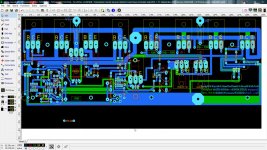
Unfortunately after drilling the Board which should be assembled, I saw some minor layout flaws, which made me, instead of assemble it, redraw the Layout one more time, thus delaying the assembling and the board already drilled, is used as reference PCB only.
So, the new layout of the board is almost finished and right now it's in rechecking phase, so that all the tracks are connected, no short circuits occur or other faults can be found and it should be RTM *ready to manufacture* later today. Hopefully I can manufacture the PCB tomorrow, another Sunday Job..
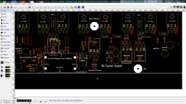
This Layout I have drawn so 3 different Drive Transistor can be used and this even with different pin layout.
So I got you a few pictures of this..
Drive Transistors BD139 are used. Input BC 559C is used, output 8x MJl4281
Hi Guys,
Here, actually should start the Part of Assembling the board..
Unfortunately after drilling the Board which should be assembled, I saw some minor layout flaws, which made me, instead of assemble it, redraw the Layout one more time, thus delaying the assembling and the board already drilled, is used as reference PCB only.
So, the new layout of the board is almost finished and right now it's in rechecking phase, so that all the tracks are connected, no short circuits occur or other faults can be found and it should be RTM *ready to manufacture* later today. Hopefully I can manufacture the PCB tomorrow, another Sunday Job..
This Layout I have drawn so 3 different Drive Transistor can be used and this even with different pin layout.
So I got you a few pictures of this..
Drive Transistors BD139 are used. Input BC 559C is used, output 8x MJl4281
Attachments


Ain´t that the Truth.Here, actually should start the Part of Assembling the board..
Unfortunately after drilling the Board which should be assembled, I saw some minor layout flaws, which made me, instead of assemble it, redraw the Layout one more time,
Against current trend, unless vey complex (multilayers, goldplating, hair thin tracks) , i prefer to home make PCBs, at least PROTOTYPES, for that very reason.
Designs are INTERACTIVE.
And even if they are "perfect" electrically from day 1, there´s layout problems, grounding issues, feedthrough, undesired interactions, or simply parts supplied not matching Sofware Library footprints so most designs, even by experienced designers, often need adjustments.
* You ordered from China, will certainly get excellent quality PCBs (no doubt about that) and for a good price, BUT there´s 10-15 day delays involved for each order (7 days is exceptional), you order a bunch, at least 5-10 since you will pay same shipping cost anyway and they have those promotions .... and on assembly you find you need some changes 😡
What to do?
Redesign: check.
Reorder: of course.
How many? .... 5-10 again? 😕
Wait another 7-10-15 days? 🙄
Pay Shipping again? 🙄
OR: use what you received, but with tracks cut here and there, parts piggybacked on others or hanging on solder side, etc.
It scratches me the wrong way.
OR:
* homemade , still in a reasonably PRO way, redesigns carried to PCBs to assembly in a couple hours or an afternoon, what´s not to like?
Redesign and tweak to your heart´s content, and when 110% certain, then you order the "fancy" ones 🙂
My point: there is still ample justification for amall scale home production, specially if new designs.
Yes, you are completely right..
And if there is a need to redraw it one more time then I will do that..
On double side cost me 10 Bucks.
So what? But I get the board when I need and more important when I want it..
and I want it NOW. (this is a Queen Phrase from late Freddy Mercury) in fact he sings, and I want it all... Same thing..
Not that the board I made is useless, No need to cut tracks, or piggy pack or likewise,, but I drew the last few days, covers my IDEAS BETTER..
Guys Will be back with the last version tomorrow, meaning the finished etched boards.
I think we both are close to each other if it comes to age.. 69 this year.. next month
It's two months for me.
I also started in the 60's with the magic pen and some etchant from Radio Shack. That turned into tape, mylar, a darkroom, and some home brewed chemical mixes in the 70's. This lasted until the early 90's when I bought the DOS version of Eagle (V2.6).
If I'm making a prototype, a one or two off, or I just want it now, I use the toner transfer method and some Ferric Chloride from Amazon or Ebay.
For anything I sell I use a PC board house. I used a US based PCB house for 14 years with good results, but when they screwed up 3 out of my last 4 orders, I switched to JLC.
Some say that the DIY boards will degrade over time and begin to self destruct in a few years. The board on the left was a prototype of the Tubelab SE board that became my first product. It was made over 16 years ago and still works fine. The board on the right is from the US board house and is about 10 years old. Both will likely outlive me.
All are DIY no matter what anyone else says. I spent 41 years working for Motorola designing cell phones and two way radios. The PCB is considered to be just another component in the product no matter who made it.
Attachments
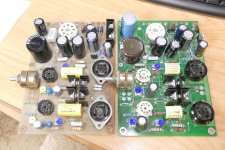
Nice, expensive Caps on the right one.. similar to Sideral or Wonder Caps.. in that time back when I lived in Asia, these were to buy with Gold only... lol
I have them still in my SP9 Audio Research Pre Amp..
You certainly did a Good and nice job..
Not every body is that open minded as you are.. Sometimes I read things, that I must rethink if I rather quit here or stay further on.. Eyesight as tight as an 2mm wide, and 1 km long line.. figure it out what I mean with this..
I think tomorrow the board, are finished and ready to assemble.. Have checked it real good 3 - for time, I hate to mess up..
Enjoy weekend..
Nice, expensive Caps on the right one.. similar to Sideral or Wonder Caps.. in that time back when I lived in Asia, these were to buy with Gold only... lol
If you look carefully at the old board on the left you will see that the coupling caps ARE Wonder Caps. I got a whole bag of used ones on Ebay cheap. They were pulled from some kind of early vintage switch mode power supply, obviously a long time ago. Most were Rel-Caps, some were Wonder Caps, both are the same thing, different market, and price. Internally there were three separate Mylar and foil rolls all wired in parallel to lessen the chances of a totally open cap.
Yea I noted that about the Wonder..
It's 6:15 Pm Now just returned from work at our Business. Weekend is close-up, but I need to clean up my Office and Manufacturing room at once.. otherwise tomorrow no Sunday work.. Want to assemble the board, get done with that AMP which these are made for, and then there is the final Project, the last one
Class A Single End - Line drive with Class A Single Ended Phone Pre Amp - TUBE.
the Phone Amp I think I need to buy because I have no IDEA at all when it comes to Tubes.. Time will tell. Project time is 1 Year, to finish before my 70'iest Birthday next year. LOL and I haven't even started yet.. Or say it like this..
The circuit is drawn and Tested but lineout is not done yet.
the case I had made special - to my Needs, at least part wise designed by me - front plate is 100% by me.
With Alps Motorized Remote Control Volumes Alps Balance Control, Alps 4 Channel Stereo Selector.. External PSU Vrail +- 55Volts that is the max I can make without breaking the transistors.. this is for the Line Drive, I like to get something like 20RMS into 600Ohms..or better 20RMS into 200Ohm Load just to keep it stable..and of course 10hz - 250Khz +- 0db
Almost no negative Feedback..
But first this last Class A has to be finished.. and to do that I need to get my Office, workroom, test room cleaned up...
Last edited:
Opemindedness is directly related to Real World Experience.Not every body is that open minded as you are.
Those who have to send a finished product through the door will be very flexible about components and techniques used, as long as they *work* properly of course.
Those who only "read" but not much else, tend to be way more "strict" and single-minded.
Oh well.
PS: LOVED:
and an excellent example: once it was perfected , (which might take 2 to 10 iterations or touchups, who knows?) THEN ordering any amount at a Commercial supplier is easy peasy ... and safe.
I silkscreen mine, so besides functional artwork can also easily add parts text ("silkscreen"), solder mask, etc.
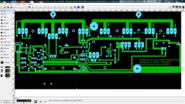
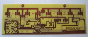
New PCB ready
New board has been done "Perfect" and in the middle of the Work, when the I finished with exposure and also developing I saw another thing which could be improved. But this I leave for a later time.. LOL
Even it's not a major change to the Circuit, it will save money in manufacturing the Boards, and this just because making the board 0.5cm or 5mm or 0.1968" inch
This would allow me to make to boards out of 1 300*210 PCB I buy..
I will leftover of 300*100 now will look if I can squeeze that to fit that size..
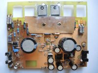
BTW this is the new Board, as it came out of washing after etching..
Finally, the next section of this will be Controlling the board and then Assembling the board
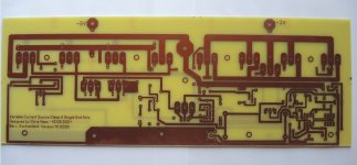
Also a Picture of a Double Sided PCB made in December 2020 also Class A just for testing, some parts of the circuit.. and this on with Ground Plane on Top side..
Have nice Sunday everybody..
Kind Regards
Chris
New board has been done "Perfect" and in the middle of the Work, when the I finished with exposure and also developing I saw another thing which could be improved. But this I leave for a later time.. LOL
Even it's not a major change to the Circuit, it will save money in manufacturing the Boards, and this just because making the board 0.5cm or 5mm or 0.1968" inch
This would allow me to make to boards out of 1 300*210 PCB I buy..
I will leftover of 300*100 now will look if I can squeeze that to fit that size..
BTW this is the new Board, as it came out of washing after etching..
Finally, the next section of this will be Controlling the board and then Assembling the board
Also a Picture of a Double Sided PCB made in December 2020 also Class A just for testing, some parts of the circuit.. and this on with Ground Plane on Top side..
Have nice Sunday everybody..
Kind Regards
Chris
Attachments
Last edited:
Nice, but it automates the wrong part of the process. It doesn't matter if I push
the spring-loaded handle or a button.
The time is lost when I try to center the drill bit above the pad. It is really hard
to see for 0.35mm holes with the tiny rest ring. 0.35mm for vias with wrapping wire.
I can drill much faster using the machine than my drill press but then again the press I've got is massive affair with a black and decker drill in it.
I do not use drills that fine normally I go with 1mm or 0.8mm. Maybe with finer drills and tiny pads it would take longer to line up. With the automated machine I can hold the PCB with two hands though Vs needing one hand to operate the press and when I have a lot to drill my arm used to get tired constantly operating the press.
Hey!! KILLER machine!!!
And I see you stretched 3D printing limits way beyond what´s normal.
I am used to seeing smallish items, whould never had thought about large thick structural I-Beams.
One doubt: I recognize Z axis movement (raising/lowering drill) but no X/Y movement6s.
Do you move PCB by hand where it´s needed?
Maybe you´d like to add a small spot or two to have a circle of bright light around the actual drilling spot.
It certainly helps my eyesight 🙂
Thanks
Yeah I hold and move the PCB by hand. When I drill I do it at the area I solder at and I've already got large amounts of light there 😀
The 3D printing definitely took a moment to understand to get to the point where I can print such things with success.
- Home
- Design & Build
- Construction Tips
- Making a double Sided PCB Guide - how it could be done..