Hello,
I have recently been working on a clocked Class-D hi-fi amplifier with the goal of using relatively inexpensive, off-the-shelf components. I decided to start this thread as a way to share my work with the DIY audio community, whilst simultaneously getting feedback from more experienced amp designers. The eventual aim is simply to produce a fine example of a clocked class D amplifier built out of discrete components.

The schematics I am posting today are very much a work-in-progress. This amplifier currently exists as a tangle of wires and components spanning several breadboards on the desk in my living room. Having said that, the amplifier does work and sounds surprisingly good to my untrained ear - it is certainly on a par with my little Lepai TA-2020 which I use as a 'reference' amplifier.
I should probably point out a couple of things before we get started:
- I am just starting out in the world of DIY audio, and especially class D amplifiers. I have never liked the inefficiency of class A and AB amplifiers, and especially not the need for large, heavy heatsinks, so in my mind the 'holy grail' is a class D amplifier which can do the same job as a conventional amplifier but without the bulk.
- I am not trying to compete with any commercial product here, or indeed with anyone else's DIY design. I am aware there are a multitude of other designs out there, including self-oscillating ones (see below), but I wanted to do it myself.
- I am not an 'audiophile'. I'm as deaf as a post from a misspent youth going to raves and playing in bands. I would love for someone with better ears than me to build this amp and tell me what it sounds like to them.
Technical considerations:
- Theoretical max output power: 18 watts on a 12 volt supply. (See "Output power")
- Full bridge complimentary output stage
- THD? Absolutely no idea. I do not have the facility to measure this. It sounds OK to me.
- This design is clocked rather than self-oscillating. I am aware that self oscillating amps can be just as good, but in my own mind I just don't like the idea. Call me crazy if you like.
- As of the date of this post (26/10/2013) there is no output filter on this amp. I have been testing the amp without - after all, no-one can hear the 500kHz switching frequency - but you should not even think of actually using this design until this has been resolved.
Output filter now added.
Firstly, I'd like to run through the basic concept. I have borrowed an image from Wikipedia to save me from drawing a block diagram, as this illustrates the basic topology of this amp rather well.

Block diagram
The first block is the modulator section.
A triangle wave is generated at ~500kHz.
The input signal at line level is first fed into a pre-amplifier. The pre-amplifier amplifies this signal so its voltage swing matches that of the triangular wave signal.
The audio signal and triangular wave are both fed into a comparator, which creates a variable duty cycle ("Pulse Width Modulated") square wave at the frequency of the triangle wave, containing the original audio data.
The square wave is fed into the output stage, where it is amplified and sent (through an output filter, to remove the high frequency component) into a speaker.
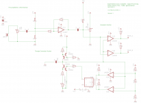
I will now explain the design in greater depth, starting with the modulator section. The full-size versions of these schematics are attached to this post.

Modulator
The modulator consists of three main sections:
Triangular Wave Generator
The triangle wave generator is somewhat more complex than expected - it turns out that generating a nice clean triangle wave at 500kHz is rather difficult. You cannot use the classic two-op-amp triangle wave generator circuit because most op-amps are simply not fast enough - in the end I went with my own take on an idea that I'm sure I saw posted somewhere in these pages (unfortunately I can't find it now!)
In brief:
- Q1, Q2 and R8 make an always-on current source which charges the timing capacitor - C4 - linearly.
- When the voltage on the capacitor reaches the upper threshold point defined by the voltage divider made up of R14, R15, R16, the comparator IC3A switches HIGH, triggering the 'Set' input of the flip flop IC4A. (The two comparators and the flip flop can be seen as a Schmitt trigger).
- T1, T2 and the variable resistor form an adjustable current sink, which is activated by the flip-flop's output. The variable resistor needs to be adjusted so the current sink passes twice the current through R8, causing the capacitor to discharge linearly at the same rate as it charged.
- When the voltage on the capacitor falls to the lower threshold point defined by the voltage divider, the comparator IC3B switches HIGH, triggering the 'Reset' input of the flip flop. This switches off the current source.
- The capacitor is allowed to charge again and the cycle repeats indefinitely.
This section produces a very clean square wave of slightly less than 500kHz.
The trigger levels are approximately 1/3 Vcc lower and 2/3 Vcc upper.
R11 is just to stop you from blowing up the current sink if you tweak the value of the pot too low.
Pre-amplifier and DC bias

This section has three functions.
1. IC1A is an op-amp configured as an inverting amplifier. It amplifies the peak-to-peak level of the input signal to match the upper and lower bounds as shown in the diagram. The closer the peak-to-peak level of the amplified signal is to these bounds, the higher the duty cycle swing of the amplifier and the louder the output signal will be. Obviously the signal must never be allowed to meet or exceed these bounds or the amplifier will clip.
2. The output of the pre-amplifier is then AC coupled and fed through a bias network consisting of the pot "OFFSET1". The pot is adjusted so that the DC offset is equal to approximately 1/2 Vcc. The adjustment of the offset level is imperative - the amplifier must be set to run as close as possible to 50% duty cycle at idle, so that the averaged current flow through the speaker is zero.
3. Negative feedback is added to the pre-amp output (see the "Feedback" section further down). This improves linearity and reduces distortion.
Modulator

Producing a PWM signal from a triangle wave - image credit: Wikipedia
The triangle wave and amplified input signal are now fed into the dual comparator IC2A and IC2B to produce a PWM signal. The illustration above gives a clearer picture of the exact mechanism of the PWM signal generation (note that this image shows a sawtooth wave instead of a triangle, but the mechanism is the same in both cases).
Both halves of this IC are used so that both an inverting and non-inverting signal can be produced to drive the output stage.
Pullup resistors R12 and R13 are necessary due to the open-collector outputs of the LM393 comparator.
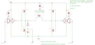
The output stage

The full-bridge output stage
Semiconductors
The output stage uses two P- and two N- channel MOSFETs. The IRFZ24N and IRF9Z24N devices were chosen due to relatively low cost and easy availability - I can see no reason why any other devices can't be used, so long as they have low gate charge and relatively low RDSon.
The MOSFETs are switched using Microchip TC4420 gate drivers. These are non-inverting drivers, hence the need for two drive signals 180 degrees out of phase. (See "To-Do" for more on this).
Other considerations
C5 serves an important function to prevent excessive power supply ripple. The value of 1000uF was chosen arbitarily and seems to work on my prototype - it may be prudent to add more filter capacitance here.
C6 and C7 must be as close to the gate driver as possible - driving the FET gates requires high current due to the capacitive nature of the gates.
Feedback
R3 and C4 form a low-pass filter to return negative feedback to the preamp stage. Again, the values here were chosen as a 'quick-fix' - the amplifier could possibly benefit from tweaking these values. I don't even know if the feedback network as I have configured it is technically correct - I just know that it seems to improve the sound noticeably. 🙂
Output Filter
I am not too familiar with the strong points of LC filter design, so I have chosen a Butterworth filter with whatever components I had to hand that seemed to work. Capacitors are film types and the inductors are two toroids wound with seven turns each. Anyone that feels like doing so may wish to adjust these values - please tell me what works for you.
Building it:
You can build this amplifier on a breadboard - despite the high frequencies involved, the circuit seems to be quite stable set up like this. I do hope to eventually produce PCB designs for this amp, but at this stage to do so would be foolhardy - I'm sure there are lots of improvements still to be made.
Here are some important considerations if you do build this design:
Supply voltage
Firstly, the TC4420s (and other Microchip drivers) are only rated to 18 volts absolute maximum. The circuit seems quite happy at 12-15 volts; I have not tested at higher voltages and would not want to go much above 15.
If you want much more output power, it will of course be necessary to climb this particular obstacle - the output stage will need to be redesigned with higher voltage rated switches (the IRFZ24N/IRF9Z24N are only rated to 55 volts VDS anyway) and a better gate driving scheme. The amp as I have built it does seem quite happy driving an 8 ohm speaker at a very acceptable level of volume, though.
Please try and use a regulated power supply if you can and make sure there is plenty of filter capacitance.
Setup
The procedure I use for setting up the amp is as follows.
1. Don't connect a speaker yet! Power on and, using a scope, check the triangle wave generator is oscillating. Adjust the SYMMETRY pot for equal rise and fall times on the triangle wave.
2. Adjust the DC offset using the OFFSET pot so that it is half the supply voltage.
3. Adjust the gain of the preamp if necessary by changing R4. It helps to scope both the + and - inputs to IC2A whilst feeding a sine wave into the input with the volume control set to max. Adjust the gain so that the peaks of the sine wave are just under the peaks of the triangle wave (see the diagram under "Pre-amplifier and DC bias" for a visual representation).
4. Connect a speaker and play music!
The 4.7k feedback resistor might need to be adjusted depending on supply voltage. If the amp distorts, try decreasing the feedback resistor value. You need to readjust the DC offset after doing this as it also has the effect of adding extra DC offset to the preamp output.
Known Problems:
- Ringing on the gate drive waveform. Can probably be helped somewhat by adding series resistors to the gate driver outputs.
To do:
- The two voltage dividers are built with 1k resistors and this is probably too low - the resistors do run slightly warm and I'm sure this isn't helping power efficiency in any way. It will be necessary to conduct tests with higher value resistors (maybe 10k instead of 1k).
- Improve the feedback network?
- The gate drivers could be replaced with a dual model with one inverting and one non-inverting driver (such as the TC4428A, or even the TC4469 which is a quad driver for a stereo amp). This would free up one half of IC2B)
- Adding some speaker protection circuitry may be an idea.
- Use faster comparators in modulator as per DUG's post, and also look at reducing the shoot-through (though this does not seem to cause a big problem right now).
Notes and other stuff:
- It's late (3am in the UK), and I'm tired. If I've missed anything or got anything wrong on the schematic, I apologise - please let me know so I can put it right. If you have any questions, just ask!
- Please do build this amp. Constructive criticism - of both the design itself and how it sounds - is welcome. I can't improve it without your help!
- This is very much a work in progress!!!!
Full-sized schematics attached below
Correction: The symmetry adjustment pot should be 1k, not 100k!
Updated 26/10/2013 - added output filter
Please see this post for the new full bridge schematic - for some reason I cannot edit the attachments on my original post.
I have recently been working on a clocked Class-D hi-fi amplifier with the goal of using relatively inexpensive, off-the-shelf components. I decided to start this thread as a way to share my work with the DIY audio community, whilst simultaneously getting feedback from more experienced amp designers. The eventual aim is simply to produce a fine example of a clocked class D amplifier built out of discrete components.
The schematics I am posting today are very much a work-in-progress. This amplifier currently exists as a tangle of wires and components spanning several breadboards on the desk in my living room. Having said that, the amplifier does work and sounds surprisingly good to my untrained ear - it is certainly on a par with my little Lepai TA-2020 which I use as a 'reference' amplifier.
I should probably point out a couple of things before we get started:
- I am just starting out in the world of DIY audio, and especially class D amplifiers. I have never liked the inefficiency of class A and AB amplifiers, and especially not the need for large, heavy heatsinks, so in my mind the 'holy grail' is a class D amplifier which can do the same job as a conventional amplifier but without the bulk.
- I am not trying to compete with any commercial product here, or indeed with anyone else's DIY design. I am aware there are a multitude of other designs out there, including self-oscillating ones (see below), but I wanted to do it myself.
- I am not an 'audiophile'. I'm as deaf as a post from a misspent youth going to raves and playing in bands. I would love for someone with better ears than me to build this amp and tell me what it sounds like to them.
Technical considerations:
- Theoretical max output power: 18 watts on a 12 volt supply. (See "Output power")
- Full bridge complimentary output stage
- THD? Absolutely no idea. I do not have the facility to measure this. It sounds OK to me.
- This design is clocked rather than self-oscillating. I am aware that self oscillating amps can be just as good, but in my own mind I just don't like the idea. Call me crazy if you like.
- As of the date of this post (26/10/2013) there is no output filter on this amp. I have been testing the amp without - after all, no-one can hear the 500kHz switching frequency - but you should not even think of actually using this design until this has been resolved.
Output filter now added.
Firstly, I'd like to run through the basic concept. I have borrowed an image from Wikipedia to save me from drawing a block diagram, as this illustrates the basic topology of this amp rather well.
Block diagram
The first block is the modulator section.
A triangle wave is generated at ~500kHz.
The input signal at line level is first fed into a pre-amplifier. The pre-amplifier amplifies this signal so its voltage swing matches that of the triangular wave signal.
The audio signal and triangular wave are both fed into a comparator, which creates a variable duty cycle ("Pulse Width Modulated") square wave at the frequency of the triangle wave, containing the original audio data.
The square wave is fed into the output stage, where it is amplified and sent (through an output filter, to remove the high frequency component) into a speaker.
I will now explain the design in greater depth, starting with the modulator section. The full-size versions of these schematics are attached to this post.
Modulator
The modulator consists of three main sections:
Triangular Wave Generator
The triangle wave generator is somewhat more complex than expected - it turns out that generating a nice clean triangle wave at 500kHz is rather difficult. You cannot use the classic two-op-amp triangle wave generator circuit because most op-amps are simply not fast enough - in the end I went with my own take on an idea that I'm sure I saw posted somewhere in these pages (unfortunately I can't find it now!)
In brief:
- Q1, Q2 and R8 make an always-on current source which charges the timing capacitor - C4 - linearly.
- When the voltage on the capacitor reaches the upper threshold point defined by the voltage divider made up of R14, R15, R16, the comparator IC3A switches HIGH, triggering the 'Set' input of the flip flop IC4A. (The two comparators and the flip flop can be seen as a Schmitt trigger).
- T1, T2 and the variable resistor form an adjustable current sink, which is activated by the flip-flop's output. The variable resistor needs to be adjusted so the current sink passes twice the current through R8, causing the capacitor to discharge linearly at the same rate as it charged.
- When the voltage on the capacitor falls to the lower threshold point defined by the voltage divider, the comparator IC3B switches HIGH, triggering the 'Reset' input of the flip flop. This switches off the current source.
- The capacitor is allowed to charge again and the cycle repeats indefinitely.
This section produces a very clean square wave of slightly less than 500kHz.
The trigger levels are approximately 1/3 Vcc lower and 2/3 Vcc upper.
R11 is just to stop you from blowing up the current sink if you tweak the value of the pot too low.
Pre-amplifier and DC bias
This section has three functions.
1. IC1A is an op-amp configured as an inverting amplifier. It amplifies the peak-to-peak level of the input signal to match the upper and lower bounds as shown in the diagram. The closer the peak-to-peak level of the amplified signal is to these bounds, the higher the duty cycle swing of the amplifier and the louder the output signal will be. Obviously the signal must never be allowed to meet or exceed these bounds or the amplifier will clip.
2. The output of the pre-amplifier is then AC coupled and fed through a bias network consisting of the pot "OFFSET1". The pot is adjusted so that the DC offset is equal to approximately 1/2 Vcc. The adjustment of the offset level is imperative - the amplifier must be set to run as close as possible to 50% duty cycle at idle, so that the averaged current flow through the speaker is zero.
3. Negative feedback is added to the pre-amp output (see the "Feedback" section further down). This improves linearity and reduces distortion.
Modulator
Producing a PWM signal from a triangle wave - image credit: Wikipedia
The triangle wave and amplified input signal are now fed into the dual comparator IC2A and IC2B to produce a PWM signal. The illustration above gives a clearer picture of the exact mechanism of the PWM signal generation (note that this image shows a sawtooth wave instead of a triangle, but the mechanism is the same in both cases).
Both halves of this IC are used so that both an inverting and non-inverting signal can be produced to drive the output stage.
Pullup resistors R12 and R13 are necessary due to the open-collector outputs of the LM393 comparator.
The output stage
The full-bridge output stage
Semiconductors
The output stage uses two P- and two N- channel MOSFETs. The IRFZ24N and IRF9Z24N devices were chosen due to relatively low cost and easy availability - I can see no reason why any other devices can't be used, so long as they have low gate charge and relatively low RDSon.
The MOSFETs are switched using Microchip TC4420 gate drivers. These are non-inverting drivers, hence the need for two drive signals 180 degrees out of phase. (See "To-Do" for more on this).
Other considerations
C5 serves an important function to prevent excessive power supply ripple. The value of 1000uF was chosen arbitarily and seems to work on my prototype - it may be prudent to add more filter capacitance here.
C6 and C7 must be as close to the gate driver as possible - driving the FET gates requires high current due to the capacitive nature of the gates.
Feedback
R3 and C4 form a low-pass filter to return negative feedback to the preamp stage. Again, the values here were chosen as a 'quick-fix' - the amplifier could possibly benefit from tweaking these values. I don't even know if the feedback network as I have configured it is technically correct - I just know that it seems to improve the sound noticeably. 🙂
Output Filter
I am not too familiar with the strong points of LC filter design, so I have chosen a Butterworth filter with whatever components I had to hand that seemed to work. Capacitors are film types and the inductors are two toroids wound with seven turns each. Anyone that feels like doing so may wish to adjust these values - please tell me what works for you.
Building it:
You can build this amplifier on a breadboard - despite the high frequencies involved, the circuit seems to be quite stable set up like this. I do hope to eventually produce PCB designs for this amp, but at this stage to do so would be foolhardy - I'm sure there are lots of improvements still to be made.
Here are some important considerations if you do build this design:
Supply voltage
Firstly, the TC4420s (and other Microchip drivers) are only rated to 18 volts absolute maximum. The circuit seems quite happy at 12-15 volts; I have not tested at higher voltages and would not want to go much above 15.
If you want much more output power, it will of course be necessary to climb this particular obstacle - the output stage will need to be redesigned with higher voltage rated switches (the IRFZ24N/IRF9Z24N are only rated to 55 volts VDS anyway) and a better gate driving scheme. The amp as I have built it does seem quite happy driving an 8 ohm speaker at a very acceptable level of volume, though.
Please try and use a regulated power supply if you can and make sure there is plenty of filter capacitance.
Setup
The procedure I use for setting up the amp is as follows.
1. Don't connect a speaker yet! Power on and, using a scope, check the triangle wave generator is oscillating. Adjust the SYMMETRY pot for equal rise and fall times on the triangle wave.
2. Adjust the DC offset using the OFFSET pot so that it is half the supply voltage.
3. Adjust the gain of the preamp if necessary by changing R4. It helps to scope both the + and - inputs to IC2A whilst feeding a sine wave into the input with the volume control set to max. Adjust the gain so that the peaks of the sine wave are just under the peaks of the triangle wave (see the diagram under "Pre-amplifier and DC bias" for a visual representation).
4. Connect a speaker and play music!
The 4.7k feedback resistor might need to be adjusted depending on supply voltage. If the amp distorts, try decreasing the feedback resistor value. You need to readjust the DC offset after doing this as it also has the effect of adding extra DC offset to the preamp output.
Known Problems:
- Ringing on the gate drive waveform. Can probably be helped somewhat by adding series resistors to the gate driver outputs.
To do:
- The two voltage dividers are built with 1k resistors and this is probably too low - the resistors do run slightly warm and I'm sure this isn't helping power efficiency in any way. It will be necessary to conduct tests with higher value resistors (maybe 10k instead of 1k).
- Improve the feedback network?
- The gate drivers could be replaced with a dual model with one inverting and one non-inverting driver (such as the TC4428A, or even the TC4469 which is a quad driver for a stereo amp). This would free up one half of IC2B)
- Adding some speaker protection circuitry may be an idea.
- Use faster comparators in modulator as per DUG's post, and also look at reducing the shoot-through (though this does not seem to cause a big problem right now).
Notes and other stuff:
- It's late (3am in the UK), and I'm tired. If I've missed anything or got anything wrong on the schematic, I apologise - please let me know so I can put it right. If you have any questions, just ask!
- Please do build this amp. Constructive criticism - of both the design itself and how it sounds - is welcome. I can't improve it without your help!
- This is very much a work in progress!!!!
Full-sized schematics attached below
Correction: The symmetry adjustment pot should be 1k, not 100k!
Updated 26/10/2013 - added output filter
Please see this post for the new full bridge schematic - for some reason I cannot edit the attachments on my original post.
Attachments
Last edited:
Interesting project.
However, some observations.
The FET's have a gate threshold of about 4.4V and 4.2V.
With a 12V supply both FET's will be on at the same time for a short period of time.
When the drive is between 4.2V and 7.6V there will be current drawn from the supply that goes directly to ground through both FET's.
My estimate (i.e. guess) is about 5A peak.
You actually have negative dead time.
This will reduce efficiency and increase power dissipation. (and stress the FET's)
The plus side (or less negative side) is that you have a high current drive that will make this current spike very short.
and
The response time for a LM393 for a low level overdrive is 1.3uS and 0.3uS for full drive.
At 500KHz that might be a little slow.
I would find something faster, but that is just me.
Have fun.
Thanks Dug - I have added these points to the 'to do' section above and I will take care of these the next time I work on the amp, especially the move to faster comparators (I have some LM311s that might be more suitable).
Today I added an output filter - I edited details into the first post, but I have attached an updated schematic for the output stage to this post as I cannot edit my attachments on the original!
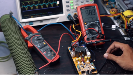
Shot of working amp on breadboard:
I have started driving a larger speaker with it - sounds good but for some reason the gate drive ICs are now getting hot. Might this be to do with the miller capacitance of the FET causing the gate to be harder to drive? I will try adding some gate resistors tomorrow and report back - I want to see if this solves the ringing problem too.
Today I added an output filter - I edited details into the first post, but I have attached an updated schematic for the output stage to this post as I cannot edit my attachments on the original!
Shot of working amp on breadboard:
I have started driving a larger speaker with it - sounds good but for some reason the gate drive ICs are now getting hot. Might this be to do with the miller capacitance of the FET causing the gate to be harder to drive? I will try adding some gate resistors tomorrow and report back - I want to see if this solves the ringing problem too.
Attachments

The drivers state 10,000pF. and an equivalent of 2.5R output resistance.
Your FET's are higher total C than that.
Look at the gate charge graphs.
Put 10R in each FET's gate. Limits gate current peaks and helps prevent Rf oscillation of the FET during OFF to ON transitions...(standard practice)
Your FET's are higher total C than that.
Look at the gate charge graphs.
Put 10R in each FET's gate. Limits gate current peaks and helps prevent Rf oscillation of the FET during OFF to ON transitions...(standard practice)
10R with a parallel diode "pointing towards" the FET driver (to slow down the start-up, but still provide a quick turn-off)
...strange...
The size of the speakers usually has not much influence on the gate drive losses.
- But stepping to higher frequencies usually does increase the gate drive losses massively.
- Also changing the supply voltage also is likely to impact the drive losses slightly.
- Filter vs. no filter might also have an impact.
Here's a question, which might sound a bit basic, but... why is the quiescent current of my amp so high with the speaker connected?
With a 50% duty cycle should I not be seeing very little power consumption at idle? Does it not work like that?
This has been kicking my a** for a few days now trying to work out something that should be rather basic.
With a 50% duty cycle should I not be seeing very little power consumption at idle? Does it not work like that?
This has been kicking my a** for a few days now trying to work out something that should be rather basic.
Here's a question, which might sound a bit basic, but... why is the quiescent current of my amp so high with the speaker connected?
With a 50% duty cycle should I not be seeing very little power consumption at idle? Does it not work like that?
This has been kicking my a** for a few days now trying to work out something that should be rather basic.
Your outputs are still driving the output filters and the drive circuitry is still charging and discharging the gates of the FET's. That power has to come from somewhere.
Efficiency comes at higher output levels because the drive power and filter power requirements don't change very much.
Look at efficiency graphs for class D amps.
What sort of quiescent current are you observing?
Sorry Stewin, I stopped working on this ages ago. Don't even have the prototype any more.
Never really got past the high quiescent current issue, but it still stands as a bit of a curiosity - a surprisingly good sounding and easy to build amp. 🙂
Never really got past the high quiescent current issue, but it still stands as a bit of a curiosity - a surprisingly good sounding and easy to build amp. 🙂
I've decided to reignite this project with the goal of building a car sub amp.
Currently in the process of testing (making a PCB this time as i no longer have the patience to build complicated circuits on breadboards!)
I have added dead time control and a few other improvements.
Will post schematics etc soon.
Currently in the process of testing (making a PCB this time as i no longer have the patience to build complicated circuits on breadboards!)
I have added dead time control and a few other improvements.
Will post schematics etc soon.
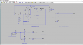
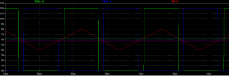
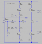
Here is an LTSpice simulation of the amp that explains my method for dead time control.
Attached asc file, a picture of the schematic and a picture of the simulation results.
I am still using LM393s for comparators at the moment but I am reducing the switching speed slightly (I am thinking 250khz is probably enough especially for a sub amp!)
There will be a new output stage designed to work at higher voltages, that is coming soon once I have built and tested the modulator.
How the dead time control works...
Essentially we are using the same triangle wave as the modulator section uses to produce an 'enable' signal based on upper and lower thresholds set by a resistive divider.
See attachment "DTU EXPLANATION"
When the triangle wave voltage goes above the upper trip point (cyan line on the graph - DTU) the comparator U3 output (DTC_U) goes HIGH.
When the triangle wave voltage goes below the lower trip point (magenta line on the graph - DTL) the comparator U4 output (DTC_L) goes HIGH.
When the triangle wave voltage is below the two trip points, both comparator outputs are LOW. This is the 'dead time'.
The size of the dead time region is controlled by adjusting R9 (set to 100 in the simulation - this will be a trimpot on the final build).
A logical AND is used to combine the DTC_U/DTC_L and non-inverting/inverting modulator outputs to create the final signals that go to the power stage. So when the DTC signals are in their LOW state, regardless of modulator output, the output signals stay low.
I hope this makes sense. I am pretty sure this will work! More to come soon.
Attachments
YMMV but...
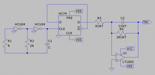
https://assets.nexperia.com/documents/data-sheet/74HCU04.pdf
https://www.rakon.com/component/docman/doc_download/223-ic-crystal-oscillator-circuits?Itemid=
Ceramic resonator or astable multivibrator from Figure 15) of the data sheet. Follow with a D Type Flop-Flip, 74HC74, then drive a rail to rail op-amp configured as an integrator to get your triangle wave.
Dead time from some more logic...
Help with class D university project
Conceptually
...
Attachments
IMHO clocked amp has less benefit compared to self osc. But only few people will agree with this.
IMHO clocked amp has less benefit compared to self osc. But only few people will agree with this.
Sure... One of your designs?
YouTube
I guess self osc done right would not suffer from extreme asymmetrical fuzz on its output but that would involve some kind of insight beyond bodging bits.
...
Attachments
Sure... One of your designs?
YouTube
I guess self osc done right would not suffer from extreme asymmetrical fuzz on its output but that would involve some kind of insight beyond bodging bits.
...
Yes he is so famous now because of yutub 🙂
Rather than people think that self oscillaton is so simple and ugly but it has advantages that self oscillation operation can adjust it self the switching duty continuously reflecting to output requirement.
At average load self oscillation will go at average speed, to give maximum clarity. At high output for example during heavy bass naturally switching speed is reduced so that the amp will produce maximum switching efficiency and full bass. Naturally your ear will not recognized that actually the amp does cheating to you because your brain will focus to the beauty of the thigh bass.
That is the reason that clocked class D is less used nowadays.
Just IMHO.
Interesting design for a triangle generator. I think for now I will stick with my design though - current source and sink and a flip flop. It is stable and predictable and one can accurately control the low and high trip points and the symmetry of the triangle wave.
I agree that self oscillating does have its beauty but I just prefer the clocked design personally.
I agree that self oscillating does have its beauty but I just prefer the clocked design personally.
Interesting design for a triangle generator.
Kind of standard wibble. In terms of accuracy, stability and repeatability it's pretty good... as good as the accuracy, 1%, of the passives plus supply variation. One other source of error might be Rdson match of the N/P channel devices in the HC74 but for a 10K load that should be minimal. The sums are easier as well.
Your current sources are going to suffer from Vbe temperature variation and switching them on and off is kind of a bad idea. A more common circuit would be
...
Attachments

- Home
- Amplifiers
- Class D
- TBJ's Class D - a discrete class D amp that anyone can build! (Work-In-Progress)