I'd like to present my old design, with double bootstrap. Now slightly refreshed and improved.
This amp allows for 200W at 4 Ohm with only +/- 45V supply. It also has very low THD: only 0.000027% 1W/1kHz and 0.0030% at 200W 1kHz (LTSpice simulation).
Older version was first published on polish DIY forum in 2010, and build by many people. This version so far is only LTSpice simulation.
Now some pictures, gain and phase:

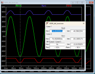
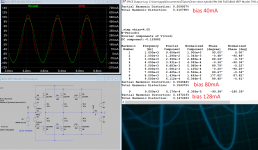
How double bootstrap works at 200W power and 10Hz, levering supply voltage for VAS by 8.2V on both rails.
Bootstrap works from very low frequency, making this design suitable for subwoofers.

This same (for single rail) taken from former (2010) version:

Overdrive response wit square pulse. Slew rate is 24V/us, and bootstrap do not causes any instability.

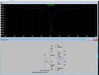
And finally schematics:

This amp allows for 200W at 4 Ohm with only +/- 45V supply. It also has very low THD: only 0.000027% 1W/1kHz and 0.0030% at 200W 1kHz (LTSpice simulation).
Older version was first published on polish DIY forum in 2010, and build by many people. This version so far is only LTSpice simulation.
Now some pictures, gain and phase:
How double bootstrap works at 200W power and 10Hz, levering supply voltage for VAS by 8.2V on both rails.
Bootstrap works from very low frequency, making this design suitable for subwoofers.
This same (for single rail) taken from former (2010) version:
Overdrive response wit square pulse. Slew rate is 24V/us, and bootstrap do not causes any instability.
And finally schematics:
Attachments
Last edited:
I see from your graph that the loop gain falls by 25dB from 1KHz to 20KHz, which implies that the THD will be 0.05% at 200W/4 ohms/20KHz.
Ed
Ed
20kHz at full power? Do you want to organize concert for bats? 🙂
Good estimation indeed, LTSpice calculates 0.043% till 9-th harmonics (180kHz).
But for 10kHz at full power it will be only 0.02% THD.
Good estimation indeed, LTSpice calculates 0.043% till 9-th harmonics (180kHz).
But for 10kHz at full power it will be only 0.02% THD.
I look at THD at 20KHz to level the playing field between amplifiers with low and high frequency dominant poles.
Ed
Ed
Look at this: without Miller compensation (without C2=5.1pF), amplifier has this characteristics

(-3dB) open loop gain bandwidth is 7kHz, and THDat 20kHz 200W is 0.038%
But such a high open gain bandwidth has also drawbacks - high harmonics have higher amplitude 🙁
(-3dB) open loop gain bandwidth is 7kHz, and THDat 20kHz 200W is 0.038%
But such a high open gain bandwidth has also drawbacks - high harmonics have higher amplitude 🙁
I expect that an EF3 will produce less distortion than the MOSFETs at full power. The frequency compensation will need adjustment.
Ed
Ed
Bias is set at 2 x 71mA. But it may be as low as 2x20mA, resulting in higher THD=0.000040% at 1W 1kHz 4 Ohm.
It depends how we define full power for different amplifiers. According to compensation I've just cut C2 to show how far it can have quite flat characteristics, and impact of this to THD. Nothing else was touched in compensation network.I expect that an EF3 will produce less distortion than the MOSFETs at full power. The frequency compensation will need adjustment.
Ed
Hi Zbyszek
I think, You set OLG too high, starting at over 90dB. From my experience it can be a bad idea. Setting OLG very high and than kill all the potential with hefty compensation. You can try some two pole compensation or output inclusive two pole compensation (invented by our collage dadod) to spread OLG nice and wide + linearize (and reduce partial gain) of two front stages of the amp. Also I would not recommend to drive two pairs of the mosfets directly from VAS stage (to high output impedance), better to simplify VAS and use some EF to drive the mosfets. Also You may have some offset issues with imbalanced input impedances at LTP input section (+ and - side of it).
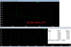
Bellow some example of very simple (single transistor input) amp with output inclusive two pole compensation at 1W and 50W @ 20kHz and 10kHz FFT's.
I think, You set OLG too high, starting at over 90dB. From my experience it can be a bad idea. Setting OLG very high and than kill all the potential with hefty compensation. You can try some two pole compensation or output inclusive two pole compensation (invented by our collage dadod) to spread OLG nice and wide + linearize (and reduce partial gain) of two front stages of the amp. Also I would not recommend to drive two pairs of the mosfets directly from VAS stage (to high output impedance), better to simplify VAS and use some EF to drive the mosfets. Also You may have some offset issues with imbalanced input impedances at LTP input section (+ and - side of it).
Bellow some example of very simple (single transistor input) amp with output inclusive two pole compensation at 1W and 50W @ 20kHz and 10kHz FFT's.
Attachments

In my simulation suite, mosfets always have more THD than some optimal biased BJTs.Just for fun, to experiment with bias and linearity of IRFP240/9240 output stage, first divergence (pierwsza pochodna vout po wejsciowym sweep).
From your experience, can any mosfet beat a pair of optimal biased MJL3281/MJL1302 in class AB?
Have you actually measured the THD? It's a lot harder to get good numbers in the lab than in the simulator. 😉
Tom
Tom
Just for fun, to experiment with bias and linearity of IRFP240/9240 output stage, first divergence (First VOUT derivative after input sweep).

Please make sure all your content is in English.
Just for fun, to experiment with bias and linearity of IRFP240/9240 output stage, first divergence (First VOUT derivative after input sweep).
Mooly
Thanks for correcting me. English is not my native language, I was not sure what I was talking about 😀
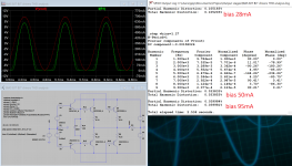
Just a few clicks (pics bellow) and it is hard to believe that mosfet OPS will beat the good BJT pair.
Matching pair, linearity, transconductance are always better in BJT. But mosfets are nice too, have a few, new, strong pairs to test.
Regards
Thanks for correcting me. English is not my native language, I was not sure what I was talking about 😀
Maybe if You have a bag of good old toshibas 2sj2012sk1530 😀In my simulation suite, mosfets always have more THD than some optimal biased BJTs.
From your experience, can any mosfet beat a pair of optimal biased MJL3281/MJL1302 in class AB?
Just a few clicks (pics bellow) and it is hard to believe that mosfet OPS will beat the good BJT pair.
Matching pair, linearity, transconductance are always better in BJT. But mosfets are nice too, have a few, new, strong pairs to test.
Regards
Attachments

As I wrote older version was built and measured (with sound card only), this mod is only simulation yet.Have you actually measured the THD? It's a lot harder to get good numbers in the lab than in the simulator. 😉
Tom
Hi, Borys, if you want to compare amplifiers, look at this:Hi Zbyszek
I think, You set OLG too high, starting at over 90dB. From my experience it can be a bad idea. Setting OLG very high and than kill all the potential with hefty compensation. You can try some two pole compensation or output inclusive two pole compensation (invented by our collage dadod) to spread OLG nice and wide + linearize (and reduce partial gain) of two front stages of the amp. Also I would not recommend to drive two pairs of the mosfets directly from VAS stage (to high output impedance), better to simplify VAS and use some EF to drive the mosfets. Also You may have some offset issues with imbalanced input impedances at LTP input section (+ and - side of it).
Bellow some example of very simple (single transistor input) amp with output inclusive two pole compensation at 1W and 50W @ 20kHz and 10kHz FFT's.
I'd like to present my project of power amplifier with novelty (I hope) gain-frequency compensation, and some other tricks resulting with high amplifier gain and very low THD.
Everybody knows most common method of making amplifier stable – it is Miller compensation: capacitor put between output and inverting input of amplifier (across one or more of amplifier’s stages). This simply puts dominant pole at very low frequency producing well known phase-amplitude open loop response of the amplifier, when high gain is flat to frequencies at most hundreds of Hertz (first, dominant pole), and...
Everybody knows most common method of making amplifier stable – it is Miller compensation: capacitor put between output and inverting input of amplifier (across one or more of amplifier’s stages). This simply puts dominant pole at very low frequency producing well known phase-amplitude open loop response of the amplifier, when high gain is flat to frequencies at most hundreds of Hertz (first, dominant pole), and...
- Zbig
- Replies: 69
- Forum: Solid State
I've compared both buffered and not-buffered VAS and decided to use non-buffered.
You are talking about DC offset or AC imbalance, because you mention impedance. not resistance.
Your comparison is for voltage-driven outputs (zero source internal resistance), but VAS has current driven output (high output resistance), so compare these circuits driven by current sources with parallel resistance of 100k, which will be much closer to VAS output than pure voltage source:(...) it is hard to believe that mosfet OPS will beat the good BJT pair (...).
And result for 10V output 1kHz, 50mA bias (each transistor) is that:
Now results are closer to each other (and second harmonics is even smaller in MOSFET). Btw. BJT requires +40% more current swing to reach 10V output.
An EF3 will be close to a voltage source. Increase the bias to 100mA per transistor and measure the THD at 30V peak.
Ed
Ed
But EF3 is still "powered" by VAS (two coupled collectors: NPN and PNP), so it is still close to current source. Of course we may argue about value of the VAS output resistance/impedance.
Here results for 30V 100mA bias:

In this case MOSFET outperforms BJT, although some harmonics are higher and some are lower. Especially 2nd is higher in BJT, and higher harmonics are bigger in MOSFET.
Here is amp/phase comparision:

BJT has first pole at 100kHz (2nd at 1MHz) and steep slope, where MOSFET has single pole at 6kHz (with 100k source's resistance) with -6dB/octave slope.
Here results for 30V 100mA bias:
In this case MOSFET outperforms BJT, although some harmonics are higher and some are lower. Especially 2nd is higher in BJT, and higher harmonics are bigger in MOSFET.
Here is amp/phase comparision:
BJT has first pole at 100kHz (2nd at 1MHz) and steep slope, where MOSFET has single pole at 6kHz (with 100k source's resistance) with -6dB/octave slope.
The 50K VAS impedance divided by two stages of emitter followers gives 5 ohms to the bases of the output transistors. I am simulating only the output BJTs. I am seeing 0.05% THD at 32 volts peak into 4 ohms.
Ed
Ed
Try to simulate ALL emitter followers, driven by high impedance VAS output. Each of them introduces distortions, and moreover, each stage has some characteristics of hfe (current gain) in a function of its collector current, which is also a source of distorition.
To make picture complete, I've added buffered MOSFET to this comparision:


So buffered MOS outperforms BJT and non-buffered MOS output stage.
To make picture complete, I've added buffered MOSFET to this comparision:
So buffered MOS outperforms BJT and non-buffered MOS output stage.
Last edited:
- Home
- Amplifiers
- Solid State
- Zbig4-DB: 200W 0.000027%THD high efficiency amplifier with double bootstrap