Exactly. The // resistor linearises the pot. I don't see it having much to do with the flattness of the thd curve though. The end result is an idle current /dead-time adjustment, exactly like Kartino proposed.
Now, guess what the second pot on the UCD700 is for 🙂
Now, guess what the second pot on the UCD700 is for 🙂
Pot on UCD400
Dear Chris,
I have never tested a UCD700 so I cannot comment what the second pot is for.
The pot on the UCD DOES affect THD quite a lot. There is a "null" setting where THD is the lowest.
Dear Chris,
I have never tested a UCD700 so I cannot comment what the second pot is for.
The pot on the UCD DOES affect THD quite a lot. There is a "null" setting where THD is the lowest.
Hi all,
As promised before,
Actually I make two plan for higher power "UcD". Firts use parallel mosfet for higher current rating. But poeple said it is not good?
Okay, then I make higher voltage rail.
During making this simulation, I have idea to make simpler comparator but works faster. IMHO I use less active parts, that no many switching inside.
Well, the result as attached. It works very good in simulation. Higher speed, almost no current crossing, and very good gate voltage form. No strength spikes at all. Even I add voltage rail to 100V!
I think it will be great if it is sucessfully on real. Especially for party dreamer! PA... It is promised for power over 1kW.
Anyway, I have no plan to make real circuit at near time. I am so busy.
Any comment are pleased.
Attachments
Hi Kartino,
Some nice work there. It's a nice simulation. On the other hand, I think 100V is the ragged edge for it, before self destruction. Even this might be too much if it happens to clip at the upper rail for too long, that upper comparator output is going to let the smoke out.
In some ways that comparator does work better. In other ways.. it's far lest robust. Does it need to be faster? The precision however is a definite bonus, something to work from. As far as less active parts... we're talking pennies here.
Those // diodes across the mosfets are really doing nothing, even in the simulation. They'd do even less in a real circuit because of parasitic inductance. If you want you can use two more diodes and disable the body diodes, far more effective.
The reason not to // mosfets, well, it shouldn't really be required at these levels if you select a good mosfet with low Ron, and of course, this style of gate driver wouldn't handle that kind of load very well. Kind of a catch-22.
Regards,
Chris
Hi Chris, can't sleep?
Actually I mean faster is at around 300khz with good form and less cross current. With this simulation, it may use moderate voltage 70V-80V with no problem, especially for comparator, is it?
Actually for parallel mosfet I already make a simulation too.
Which one that better promised for higher power? The higher voltage rail or paralleing mosfets?
Thanks and regards,
kartino
Attachments
comparator at clip
Hi Chris,
Can I use passive resistor for limiting current when clip occur? For example the max. current limited by R19 = 20k for 100V rails is 200/20000 = 10mA? (Sorry I didn't get the point, if you mentioned that comparator will smoked at clipping caused by over load ...?)
regards,
kartino
Hi Chris,
Can I use passive resistor for limiting current when clip occur? For example the max. current limited by R19 = 20k for 100V rails is 200/20000 = 10mA? (Sorry I didn't get the point, if you mentioned that comparator will smoked at clipping caused by over load ...?)
regards,
kartino
Kartino, I take a few things back.
I think in the end precision and adjustability thereof takes a big hit with this comparator, I think it has alot less gain too, and slower switching overall. For the cost of a few parts... I can't imagine the PSRR of the lower rail being very good with it either? It sure doesn't look like it, any signal applied to the lower rail modulates the output nicely.
I still don't think the drivers will survive in a practical setup, but I think the comparator might. It's hard to say at a glance. Q6 will be running far hotter than Q7 though, near it's limite. That's the point to the the cascode, to move the extra dissipation of the high side output away from the comparing portion, no current hogging can occure. Far more important at higher voltage.
I've had my version of it working well over 500kHz, if you're finding it slow, it's very likely due to the transistor selection!
You possibly have a nice simplification for a low powered version, I sure would not recommend this at 100V rails, or anywhere near it.
The version of comparator used in your // mosfet version got me some good results when I experimented with it. I had the same kind of idea in mind that I think you do. However I found that properly biased / loaded, the active biased diode cascode always had a bit of an edge, and it really gets no simpler. My other tweak for that is to use the CB diode in the same manner.
I don't think I'd try building this, but if you do I'd love to hear of your results.
Best Regards,
Chris
First design (with more complex comparator) is MUCH better.
About last one: there is no need of R19C14C15
C9C10 can be eliminated. If you need to lower hf gain, you can use 1 (one) cap across Q6Q7`s bases.
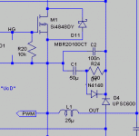
D11D12 have very big parasitic capacitance, can be substituted with 5A Shottky (btw, for +\-100V rails you MUST use 250V+ superfast diodes, like SF56).
So.. I don`t think that the last design would live long enought to hear them 🙄
About last one: there is no need of R19C14C15
C9C10 can be eliminated. If you need to lower hf gain, you can use 1 (one) cap across Q6Q7`s bases.
D11D12 have very big parasitic capacitance, can be substituted with 5A Shottky (btw, for +\-100V rails you MUST use 250V+ superfast diodes, like SF56).
So.. I don`t think that the last design would live long enought to hear them 🙄
I have some comments about some of the parts.
D8, D10 and D5 looks like a protection feature, but they aren't really doing anything, because V4 is always 12V. In practice wouldn't it be enough to clamp V4?
D1 and D3 are really doing nothing. They are placed in parralel with Q3 and Q10's internal diodes (remember it's PNP or NPN, so a BJT has two internal diodes, where the one is included in the part symbol).
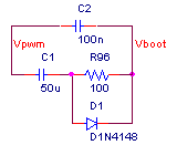
The size of C1 is crazy. It should at least be connected in series with a resistor, to prevent failure of D4. Placing a diode over this resistor, will do the job you probably intended (see the attached picture).
Whay do you need the complex configuration of the noninverting input on the comperator? Wouldn't 60k//<some large cap> do the job? The bias current is provided by 60k and the cap clamps the voltage a high frequencys. Right now the noninverting input has an ugly waveform on it. So your reference is an ugly waveform.
Anyway it's a interesting to see this high voltage UCD in the simulator. As mentioned before, a practial amp would require some attention to power dessapation in the components, but one thing at a time.
D8, D10 and D5 looks like a protection feature, but they aren't really doing anything, because V4 is always 12V. In practice wouldn't it be enough to clamp V4?
D1 and D3 are really doing nothing. They are placed in parralel with Q3 and Q10's internal diodes (remember it's PNP or NPN, so a BJT has two internal diodes, where the one is included in the part symbol).
The size of C1 is crazy. It should at least be connected in series with a resistor, to prevent failure of D4. Placing a diode over this resistor, will do the job you probably intended (see the attached picture).
Whay do you need the complex configuration of the noninverting input on the comperator? Wouldn't 60k//<some large cap> do the job? The bias current is provided by 60k and the cap clamps the voltage a high frequencys. Right now the noninverting input has an ugly waveform on it. So your reference is an ugly waveform.
Anyway it's a interesting to see this high voltage UCD in the simulator. As mentioned before, a practial amp would require some attention to power dessapation in the components, but one thing at a time.
Attachments
Kuzmenko said:First design (with more complex comparator) is MUCH better.
But we should certainly not discourage experimentation! I commend him for it. Don't be so quick to dismiss what I've given you though.
Kuzmenko said:About last one: there is no need of R19C14C15
C9C10 can be eliminated. If you need to lower hf gain, you can use 1 (one) cap across Q6Q7`s bases.
Totally agree.
Kuzmenko said:D11D12 have very big parasitic capacitance, can be substituted with 5A Shottky (btw, for +\-100V rails you MUST use 250V+ superfast diodes, like SF56)
Schottky's have a rather high capacitance to begin with. Bruno has shown in the past that the parasitic inductance renders this idea all but useless, the body diode saturates well before the schottky can turn on. The only way I can see it possibly helping is the parasitic capacitance it adds to the switching node helps slow the slew rate of the switching node, possibly helping the body diode by giving it more time to turn off.
A fast rectifier is typically no good in // to the body diode either, still a higher forward drop than the body diode of the types of mosfet we want to be using in this kind of application.
Either select the perfect mosfet that doesnt' require it, or use an anti-series diode as well to turn off the body diode as I've shown in this thread someplace.
Sovadk, you're right about C1 being too small 🙂 The bigger mistake is it's missing a diode before Q10. Personally I'd try and make due without a resistor here, your rendition of it doens't make sense to me at all. I guess I'd have to see it implemented.
I have to say, I've spent probably more than a few hundred hours working on my version of it, you can benefit from that if you so chose, because I've already done all this kind of stuff for you, or, you can go down this route. 😕
Regards,
Chris
2sovadk:
C1 is crazy big or crazy small? 😀
I`m use for flying supply good 330uF, and 1A Shottky as D4. It works for now. For understanding of complex non- inv. input circuit take excurse in nov.2005 and look at initial design 😉
D1D3 must be Shottky diodes. Again, please see initial design.
C1 is crazy big or crazy small? 😀
I`m use for flying supply good 330uF, and 1A Shottky as D4. It works for now. For understanding of complex non- inv. input circuit take excurse in nov.2005 and look at initial design 😉
D1D3 must be Shottky diodes. Again, please see initial design.
Kuzmenko said:2sovadk:
C1 is crazy big or crazy small? 😀
I`m use for flying supply good 330uF, and 1A Shottky as D4. It works for now. For understanding of complex non- inv. input circuit take excurse in nov.2005 and look at initial design 😉
D1D3 must be Shottky diodes. Again, please see initial design.
Have you seen the "initial design" 🙄
Sovadk:
Regarding D5, have a look at R5, the two form a type of precharge circuit, that along with a small pause before enabling the output will ensure it can switch high when required, very much required.
I agree about D8 and D10. Alot of people consider it standard practice to use zeners at the gate, just in case. Some figure (if you do the math?) it's got the perfect amount of parasitics to form a nice resonant circuit, especially if they ever conduct and consequently turn off. As a strick protection feature.... OK... so make them >15V so they only get used in case of. Maybe it'll save the driver if a fet blows.
There should be another diode in series with R5 and proportioned such that the precharge circuit drops out once it starts switching.
On the original Hypex modules C1 was actually 100uF, now it's 220uF, sized for worst possible case, something crazy like 30% 20Hz clipping. You don't want the gate to fall too far.
Regards,
Chris
D8, D10 and D5 looks like a protection feature, but they aren't really doing anything, because V4 is always 12V. In practice wouldn't it be enough to clamp V4?
Regarding D5, have a look at R5, the two form a type of precharge circuit, that along with a small pause before enabling the output will ensure it can switch high when required, very much required.
I agree about D8 and D10. Alot of people consider it standard practice to use zeners at the gate, just in case. Some figure (if you do the math?) it's got the perfect amount of parasitics to form a nice resonant circuit, especially if they ever conduct and consequently turn off. As a strick protection feature.... OK... so make them >15V so they only get used in case of. Maybe it'll save the driver if a fet blows.
There should be another diode in series with R5 and proportioned such that the precharge circuit drops out once it starts switching.
On the original Hypex modules C1 was actually 100uF, now it's 220uF, sized for worst possible case, something crazy like 30% 20Hz clipping. You don't want the gate to fall too far.
Regards,
Chris
2classd4sure: I mean initial Kartino`s design. And you, probably, mean Bruno`s? He- he 🙂
Is there any ideas of IR2113 based UcD?😀 Not that IR`s reference monster, but much simpler and exactly IR2113.
Is there any ideas of IR2113 based UcD?😀 Not that IR`s reference monster, but much simpler and exactly IR2113.
Btw, about variable resistor between cascode and negative supply rail. I am not sure that it can be used to trim dead time, but... Hmm, ok. Rising their value will increase or decrease dead time?
sovadk said:To release the stress on D4, I've attached an implementation of the C1,C2 circuit from before.
Thanks that helped me see what you're going for. That and a few hours sleep.
Preferably one could find a diode that can take the stress, the charge pulses are of short duration after all, and we do want it to charge fast. If not I'd use that though, with a proper precharge circuit.
Kuzmenko, I didn't mean Bruno's schematic that's not available for viewing. About R1, simulate simulate simulate! 😀
Regards,
Chris
Hi, actually I am think about the accuracy of LTSpice simulation result.
The second is the high side driver, I am worry that the driver can survive at the voltage level.
For comparator, I think it will survive. I saw lots of Class AB, with that arrangement at that voltage level. Is class AB input stage work harder than class D?
For Sovadk, the charging time start stop at -rail+12V I think no worry about diode stress. Our concern is to charge the cap fastly. Not like your totem-pole BJT, this driver need more power to charge and hold the gate driver. That is the reason that we need big cap and fast charger.
For zener at gate mosfet, yes, is used for protection, work as standby, do nothing.
The non inverting input, originally this amp is balanced input. I will keep that.
OK, R19 C14 C15 is used for passive current limiter. Safety reason too. I will consider later.
So, I am worry two thing: 1) LTSpice accuracy, 2) High side driver reliability
Thanks for all suggestions,
Regards,
Kartino
- Status
- Not open for further replies.
- Home
- Amplifiers
- Class D
- yet another UcD