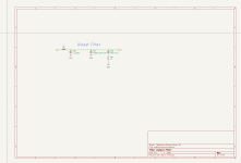
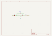
I have worked on TPA3255 based BTL amplifier for a while now. As this is my first time attempting to layout a class D amplifier I would appreciate some feedback.
I have tried to follow the layout and schematic from the EVM, the feedback given in other threads on here, as well as SLAA788A for the PFFB, but I have probably missed something.
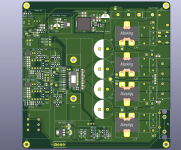
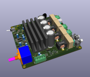
The layout is done on a two layer PCB and I will get all the SMD components assembled by the PCB manufacturer.
The VIA stitching is not done yet, so that is missing. The connectors I have mainly chosen for easy testing.
I have attached both schematics and PCB screenshots here, as well as a PDF of the schematic.
Thanks in advance!
I have tried to follow the layout and schematic from the EVM, the feedback given in other threads on here, as well as SLAA788A for the PFFB, but I have probably missed something.
The layout is done on a two layer PCB and I will get all the SMD components assembled by the PCB manufacturer.
The VIA stitching is not done yet, so that is missing. The connectors I have mainly chosen for easy testing.
I have attached both schematics and PCB screenshots here, as well as a PDF of the schematic.
Thanks in advance!
Attachments
-
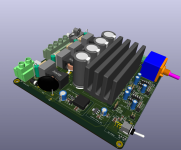 side_3d.png150.4 KB · Views: 300
 -
 tpa3255_closeup.png122.2 KB · Views: 260
 -
 front_copper.png147.2 KB · Views: 238
 -
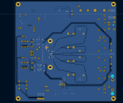 rear_copper.png66.9 KB · Views: 240
 -
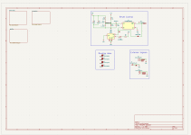 overall.png27.2 KB · Views: 241
 -
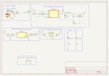 power_supply.png41.6 KB · Views: 215
 -
 inputs.png29.3 KB · Views: 224
 -
 preamplifier.png26.1 KB · Views: 236
 -
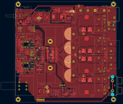
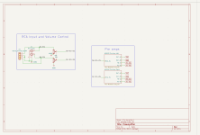
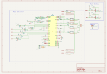 main_tpa3255.png54.1 KB · Views: 241
 -
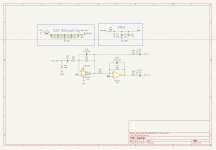
 output_filter.png15.5 KB · Views: 243
 -
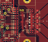
 pffb.png13.7 KB · Views: 250
 -
TPA3255_pffb_amp.pdf855 KB · Views: 215
-
 top_3d.png154.9 KB · Views: 265
 -
 top_32_no_pth.png144.1 KB · Views: 287

Hi Foxter,
Why do you say that maybe you missed something?
It seems like a good project to me, I'm surprised that no one has intervened yet.
I saw that you made some variations, such as using the LMR16006XDDCR regulator instead of the LM5010ASD/NOPB used in the EVM version, but which costs 10 times more.
The most obvious difference between the two seems to be the maximum current, 600 mA, versus 1A.
Have you considered that it is still sufficient, and possibly redundant?
The next question is:
Did you print the board and test it, or are you still waiting for feedback, before proceeding?
By the way, your pdf with the schematic is fabulous! 👍
Is it all thanks to Kicad 8 or did you use a different software?
Basically, it embeds the BOM and any details of each component.
My version of Kicad 5.1, unfortunately, does not do this.
I saw that you included the LCSC codes.
Have you already tried to calculate the estimate for the SMD assembly?
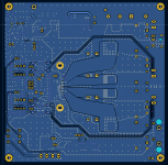
I think you kept all the SMD parts on the TOP layer.
I'm not very convinced by the Output traces that first end up on the bottom through vias, but then return to TOP just before the output inductors, again through 5 vias.
I think that these traces should have a direct path as much as possible,, on the same layer.
Then, with such a complex board, it seems more reasonable to keep both the volume potentiometer
and the RCA inputs connectors (or other direct controls, as the RESET sw) separate from the PCB.
These are components that are more easier to install on the case (on whatever case you choose).
Even more restrictive is to have them arranged front to back (Potentiometer and RCA Inputs).
In this way the case will necessarily have to be exactly as deep as the PCB.
It seems a bit too restrictive, don't you think?
Anyway, it's just my opinion.
Marco
Why do you say that maybe you missed something?
It seems like a good project to me, I'm surprised that no one has intervened yet.
I saw that you made some variations, such as using the LMR16006XDDCR regulator instead of the LM5010ASD/NOPB used in the EVM version, but which costs 10 times more.
The most obvious difference between the two seems to be the maximum current, 600 mA, versus 1A.
Have you considered that it is still sufficient, and possibly redundant?
The next question is:
Did you print the board and test it, or are you still waiting for feedback, before proceeding?
By the way, your pdf with the schematic is fabulous! 👍
Is it all thanks to Kicad 8 or did you use a different software?
Basically, it embeds the BOM and any details of each component.
My version of Kicad 5.1, unfortunately, does not do this.
I saw that you included the LCSC codes.
Have you already tried to calculate the estimate for the SMD assembly?
I think you kept all the SMD parts on the TOP layer.
I'm not very convinced by the Output traces that first end up on the bottom through vias, but then return to TOP just before the output inductors, again through 5 vias.
I think that these traces should have a direct path as much as possible,, on the same layer.
Then, with such a complex board, it seems more reasonable to keep both the volume potentiometer
and the RCA inputs connectors (or other direct controls, as the RESET sw) separate from the PCB.
These are components that are more easier to install on the case (on whatever case you choose).
Even more restrictive is to have them arranged front to back (Potentiometer and RCA Inputs).
In this way the case will necessarily have to be exactly as deep as the PCB.
It seems a bit too restrictive, don't you think?
Anyway, it's just my opinion.
Marco
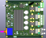
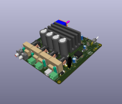
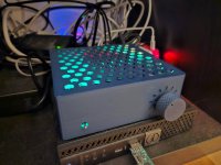
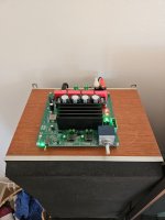
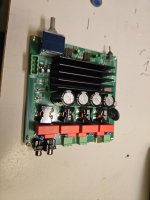
Thanks for the comments, I have in fact ordered the board and overall I am very happy with the results, (almost) everything works as expected.
I ended up coming to some of the same conclusions as you, so the final board has many more vias on the output traces.
The only real issues has been that the pin layout for the transistors for the status LEDs turned out to be wrong, but that is only cosmetic.
I used Kicad 8 for everything and ordered the board from jlcpcb with all SMD components soldered for around 80 USD before tax and shipping, and then bought the rest of the components on Digikey for around 150 USD.
The regulator choice was mostly to have a more modern component with a higher switching frequency.
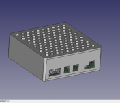
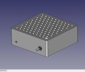
Regarding the case, I wanted to create small form factor 3D printed case, hence why I included the potentiometers and RCA directly on the PCB.
I have attached some images of the final result here.
I ended up coming to some of the same conclusions as you, so the final board has many more vias on the output traces.
The only real issues has been that the pin layout for the transistors for the status LEDs turned out to be wrong, but that is only cosmetic.
I used Kicad 8 for everything and ordered the board from jlcpcb with all SMD components soldered for around 80 USD before tax and shipping, and then bought the rest of the components on Digikey for around 150 USD.
The regulator choice was mostly to have a more modern component with a higher switching frequency.
Regarding the case, I wanted to create small form factor 3D printed case, hence why I included the potentiometers and RCA directly on the PCB.
I have attached some images of the final result here.
Attachments
-
 Screenshot from 2024-11-19 20-34-21.png45.1 KB · Views: 94
 -
 Screenshot from 2024-11-19 20-13-42.png221.8 KB · Views: 79
 -
 Screenshot from 2024-11-19 20-34-11.png34.2 KB · Views: 75
 -
 Screenshot from 2024-11-19 20-13-28.png300.5 KB · Views: 77
 -
 Screenshot from 2024-11-19 20-12-37.png172.2 KB · Views: 80
 -
 Screenshot from 2024-11-19 20-11-47.png432.3 KB · Views: 85
 -
 20241119_194108.jpg333.1 KB · Views: 97
 -
 20240503_092702.jpg451.1 KB · Views: 94
 -
 20240502_211644.jpg368.8 KB · Views: 99
 -
 20240502_193258.jpg420 KB · Views: 91
I have to say that the printed case is nice, it has a Star Wars look. 😎
I hope you have planned some air inlet holes in the base too, to ensure good circulation.
Unfortunately there are some disadvantages.
The first is that dust enters freely from above. The second (more important), is that a plastic case has no shielding power.
The third is that it is perhaps not ideal to insert a device that can tend to heat up a lot (depending on use) into a printed plastic enclosure.
And even if it does not soften or deform over time, it could emit substances that are not healthy to breathe.
...But it should not be difficult, alternatively, to find an extruded aluminum case to cut to the right size. 😉
I was rather curious to know your listening impressions, as well as to know if you have made any comparisons between the standard configuration and PFFB.