Inspired by circuitbasics.com article.
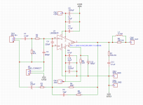
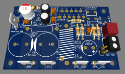
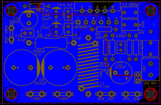
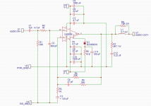
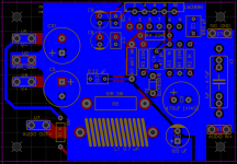
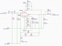
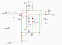
Latest revision of the LM3886 gainclone PCB:
R3, R4 - 0.1% tolerance - can be hand matched from like twenty resistors of 1% tolerance.
R7, R8 - 10 ohms:
2W Ohmite Wirewound Resistor - $1.33 - 588-WHC10RFET
3W Ohmite Wirewound Resistor - $0.79 - 588-53J10RE
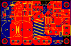
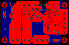
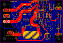
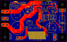
Gerber files are attached. Great website to make those boards is JLCPCB.
Latest revision of the LM3886 gainclone PCB:
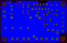
- Power ground and signal ground are two separate plains with the ability to connect together.
- Plus and minus power supply plains are doubled on both sides of the PCB for the optimal current handling.
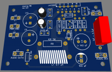
- .25 inch terminal connectors for power and speaker wires.
- Space for 5mm or 10mm lead input capacitor.
- Space for all of the optional stability components.
- Space for six supply bypass capacitors
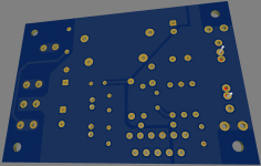
- PCB size is 70mm x 45mm.
- Four holes for mounting PCB to the heatsink with 90 degrees bracket or to the chassis.
- C1 - 2.2uF - WIMA MKS2 film capacitor - Mouser part # 505-MKS2C042201KKSSD
- C2 - 220uF - Nichicon Audio Grade Electrolytic Capacitor - 647-UFG1V221MPM
- C3 - 680pF - WIMA FKP2 film capacitor - 505-FKP2680/100/5
- C4 - 220pF - WIMA FKP2 film capacitor - 505-FKP2220/100/5
- C5 - 10pF - TDK C0G Multilayer Ceramic Capacitor - 810-FG18C0G1H220JNT0
- C6, C11 - 1000uF 50V - Nichicon Electrolytic Capacitor - 647-UPS1H102MHD
- C7, C10 - 22uF 50V - Panasonic Organic Polymer Capacitor - 667-50SEK22M
- C8, C9 - 4.7uF 50V - TDK X5R Multilayer Ceramic Capacitor - 810-FG14X5R1H475KRT6
- C12 - 100uF 50V - Nichicon Electrolytic Capacitor - 647-UVZ1H101MPD1TD
- C13 - 0.1uF 50V - TDK X7R Multilayer Ceramic Capacitor - 810-FG18X7R1H104KNT0
R3, R4 - 0.1% tolerance - can be hand matched from like twenty resistors of 1% tolerance.
R7, R8 - 10 ohms:
2W Ohmite Wirewound Resistor - $1.33 - 588-WHC10RFET
3W Ohmite Wirewound Resistor - $0.79 - 588-53J10RE
Gerber files are attached. Great website to make those boards is JLCPCB.
Attachments
Last edited:

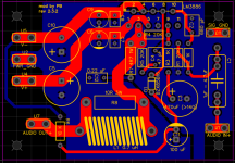
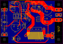
New revision 2.0:
Gerber files are attached


- Fixed mute cap polarity
- Reduced size to 55mm x 85mm
- Updated capacitors' footprint to WIMA and ceramic sizes
- Updated resistor sizes
- Added 1cm clearance for C5 and C10 from the side of the heatsink
Gerber files are attached
Attachments
push C10 and C5 5-10 mm higher .
C1 is a little bit small .
C4 is still too big.
R8 is too big , 3w is enough.
C6,c9 can be 8-10 mm diameter.
c7 and c8 could be LxW =7.5x7.5mm, 1uf 100v film caps are aprox that size
L1 is too small. L1 could be placed outside the amp board.
When using ground planes make sure you have thermal reliefs for the components .
Thank you for your input! I really appreciate it!
C4 will be ordered on Mouser - WIMA part # 505-FKP247/1000/5. According to datasheet size is 4.5W x 6H x 7.2L with 5mm PCM (mount pads). Should I use a different one?
C6, C9 - Mouser part 647-UVR2A220MED
C7, C8 - Mouser part 810-FG26X7R1H475KRT0 ceramic capacitors. Should I use film caps?
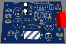
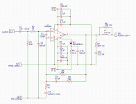
Rev 2.2 updates:


Gerber files attached
C4 will be ordered on Mouser - WIMA part # 505-FKP247/1000/5. According to datasheet size is 4.5W x 6H x 7.2L with 5mm PCM (mount pads). Should I use a different one?
C6, C9 - Mouser part 647-UVR2A220MED
C7, C8 - Mouser part 810-FG26X7R1H475KRT0 ceramic capacitors. Should I use film caps?
Rev 2.2 updates:
- C10 and C5 were pushed 5mm ish
- C1 - added 22.5mm long soldering pads, clearance is increased to 10mm for width now
- R8 downsized to 3W Mouser part number 594-AC03W10R00J
- L1 was updated to 25mm length
Gerber files attached
Attachments
Not to discourage you doing your own layout but this one works rather well:
open source lm3886
Lots of inspiration to be found there for your own layout and this thread is a real gem too:
P2P LM3886
open source lm3886
Lots of inspiration to be found there for your own layout and this thread is a real gem too:
P2P LM3886
X7r caps are great there , I would look for 100v X7R ones since their capacitance will change less than the ones rated 50v, or use film caps like mks2 , b325 or mkt370/470 63v.
The 47 pf cap .... I never tried a film one , I only used c0g ar mica ones , but the fkp cap might work well .
C6/9 SHOULD NOT be VR series caps , since you need low impedance 105C caps there , something like panasonic fk, fs, fm, fc or nichicon pm, pw or other.
For C5/ C10 is same story , low impedance 105C caps.
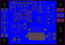
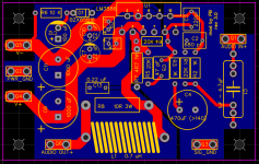
Revision 2.3:

- Updated sizes for C5, C10, C11, C3
- PCB size reduced to 55mm x 80mm
- Created parts list - for mono channel
Attachments

Rev 2.3.1:
Gerber file attached.
List of parts PDF attached.
- Updated C7, C8 footprints
- Upgraded C5, C10 caps to low esr Panasonic
Gerber file attached.
List of parts PDF attached.
Attachments
c8,c7,c6,c9 can be pushed as close as possible to the chip pins.
The trace from c8 to pin 4 needs to be wider, same as c7 to pin 1 ,
trace from pin 1 to pin 5 can be mirrored on the bottom side .
C11/d1/r10 can be relocated to the left top corner , you can make the board a little smaller this way.
How did you get to the 140uf value cap ?
The trace from c8 to pin 4 needs to be wider, same as c7 to pin 1 ,
trace from pin 1 to pin 5 can be mirrored on the bottom side .
C11/d1/r10 can be relocated to the left top corner , you can make the board a little smaller this way.
How did you get to the 140uf value cap ?
How did you get to the 140uf value cap ?
Circuitsbasics.com article
Attachments

Rev 3.2:
- Clipped leg #2 to run the V- trace. Trace size is 5mm now.
- C6, C11 are 16mm now with LS=7.5mm
- Board size is 50mm x 80mm
Attachments
Last edited:
- Home
- Amplifiers
- Chip Amps
- Yet another LM3886 gainclone PCB based on circuitbasics.com