russ:
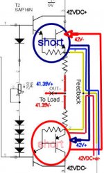
looks to me like the shorted emitter resistors no longer make a contribution to bias stability.
if that's by design, ok. 😱
but i'm guessing it's not ...
mlloyd1
looks to me like the shorted emitter resistors no longer make a contribution to bias stability.
if that's by design, ok. 😱
but i'm guessing it's not ...
mlloyd1
Hi mlloyd1,
You are right. It was simply a case of me over thinking something and missing the obvious. I am seeing the wisdom of simply taking the feedback from the load (between emitter resistors). Consider me convinced.
I will revise the schematic tomorrow. I have a few other little tweaks I made. I will likely lay the PCB out so that one can use the built in emittter resistors on the SAP16 or use their own.
Thanks to everyone for the sociable interchange of good information.
Cheers!
Russ
tiltedhalo said:
Its a mute point now man, but in any case the short you show there is still not able to get to the load unless it goes through at least one emitter resistor.
See my post above. 😎
 Cheers mate. 🙂
Updated schematic
Here is the current schematic.
I am now taking feedback from emitter resistors instead of S pins.
I also changed the THS4131 compensation cap to 200pf (C1 and C2) as I think this value should work fine and reduce the phase shift a bit. I will know better once I get a chance to test the circuit.
Cheers!
Russ
Attachments
Very Interesting design
Just an idea, one could use the Vocm input on the Ti chip
as the error input node for DC offset compensation.
(One will still have to add an additional OP-amp to implement the integrator though)
Just an idea, one could use the Vocm input on the Ti chip
as the error input node for DC offset compensation.
(One will still have to add an additional OP-amp to implement the integrator though)
Experments With Output Stages?
Hi,
Simple minded. Any experiments planned with output stages
besides 1-2-3 Darlington pairs?
Thanks for your new ideas.
Mark
Hi,
Simple minded. Any experiments planned with output stages
besides 1-2-3 Darlington pairs?
Thanks for your new ideas.
Mark
Re: Experments With Output Stages?
Hi Mark,
Yes, I am planning on testing FETs too, eventually. but probably not tubes.... 🙂 Just not really into that.
I will be providing here on the thread PDFs for PCB layouts shorty which should allow people to play with the circuit. I may not have time to actually build the circuit do to the fact I am in the midst of a move. So one of you may get to be the guinea pig. 🙂
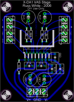
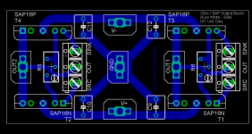
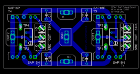
The set will consist of 3 PCBs(or more if you plan on paralleling output devices) per channel. One will be a the differential PCB (THS4131). One will be the VAS stage (4702 but could also be discrete). One will be the SAP16 output stage, which could be substituted for another PCB or even P2P wired FETs or something.
Cheers!
Russ
Mark St. Denis said:Hi,
Simple minded. Any experiments planned with output stages
besides 1-2-3 Darlington pairs?
Thanks for your new ideas.
Mark
Hi Mark,
Yes, I am planning on testing FETs too, eventually. but probably not tubes.... 🙂 Just not really into that.
I will be providing here on the thread PDFs for PCB layouts shorty which should allow people to play with the circuit. I may not have time to actually build the circuit do to the fact I am in the midst of a move. So one of you may get to be the guinea pig. 🙂
The set will consist of 3 PCBs(or more if you plan on paralleling output devices) per channel. One will be a the differential PCB (THS4131). One will be the VAS stage (4702 but could also be discrete). One will be the SAP16 output stage, which could be substituted for another PCB or even P2P wired FETs or something.
Cheers!
Russ
XELB said:Russ, can you tell me the Bias current in the output stage ?
The SAP16 datasheet say to adjust the VR between the "D" pins for 40ma which should be 2.5ma or so through the VR.

Russ,
I know that you are a busy man with a day job but ...
Have you built this amp project? It is an interesting topology. I am toying with the idea of jumping into a SUSY project based on your hard work.
Carl
I know that you are a busy man with a day job but ...
Have you built this amp project? It is an interesting topology. I am toying with the idea of jumping into a SUSY project based on your hard work.
Carl
- Status
- Not open for further replies.
- Home
- Amplifiers
- Chip Amps
- XDA-1 -- A symmetrical power amp utilizing LM4702