I just read Zen Var. - Part 4
Nice reading.
In my X-SOZ it is obvious that the impedance and the frequency respons is working at the edges, may be a problem, may be not.
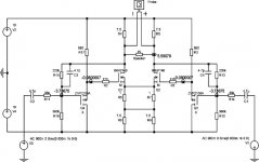
I coud not resist to give it a sim, adding "the penultimate zen" buffer to this circiut.
Tis is a quick shut, but in the sim it is clear what it can do for X_SOZ. High input impedance and exelent low and high frequency.
And may be it also will benefit from other virtues from this buffer deskribed so well by Mr. Pass.
Any comments?
I must make two posts, each for one picture.
Nice reading.
In my X-SOZ it is obvious that the impedance and the frequency respons is working at the edges, may be a problem, may be not.
I coud not resist to give it a sim, adding "the penultimate zen" buffer to this circiut.
Tis is a quick shut, but in the sim it is clear what it can do for X_SOZ. High input impedance and exelent low and high frequency.
And may be it also will benefit from other virtues from this buffer deskribed so well by Mr. Pass.
Any comments?
I must make two posts, each for one picture.

😎 It seem to be very interesting .I like to think the input buffer not as a second stage thus probably it will be a good
improvement.
These days I am enjoing the Zen -like Headphone amp (that with
an imput buffer too is eccelent) and I left soz a little aside .
Even becouse I am planning to buy more powered transformers.
By the way , what is the voltage at the output of the buffer?
Stefano
improvement.
These days I am enjoing the Zen -like Headphone amp (that with
an imput buffer too is eccelent) and I left soz a little aside .
Even becouse I am planning to buy more powered transformers.
By the way , what is the voltage at the output of the buffer?
Stefano
Hi Stefano
The voltage output from the buffer is the same as at the input since it is a follower.
The input signal presented at the node between R15 an C1 is 900mV (amplitude).
The bufferinput is 220 mA, that is at the node between the gate and R14. This lowering of the signal is caused by the NFB.
These values are just a first shut, for best performance they should be reconsiderd.
I am not shure, if the X-SOZ will benefit from these buffers, I havn´t actually builded them. I just felt, that the problems I had with the X-SOZ in a way was related to "The One And Only´s" considerations in Zen Var. 4.
I am looking foreward to rebuild my test-X-SOZ to the (final?) X-SOZ with better parts in the X-circiuit, and put some new blackgate caps into my BOSOZ.
And happy listening in your headbangers, i hope you will enjoy your X-SOZ too some day!
It was a very interesting read.
I have understood that, if the low input impedance is mostly resistive in character, it is not a problem to keep the wide bandwidth.
Meanwhile, Mr Nelson Pass comments on his article: "The Son of Zen can have any input resistor you care to use."
Why the low input impedance will make the life hard for preamps driving it...?
Look forward to hearing.
I wrote in my previus post: "The bufferinput is 220 mA".
I ment "The bufferinput is 220 mV". Sorry!
Low inputimpedance demands more current to keep the signal alive.
If you are using coupling caps in front of this input, then the value of the caps should increase with the lower inputimpedance.
This is my understanding. I am not a proffessional in these matters, so if i am wrong, i hope someone wil correct me.
Hallo Henrik and all of you,
is interestin to know if is it possible obtain a zero volt potential at
the source pin of the imput buffer (dc) . To do this the gate of this buffer there must be -4 volt .Isn't it?
I tell you this 'couse in this way the output swing will be greater.
And the pass band too.
What do you think?
Stefano
Stefano
As I understand the "Penultimate inputbuffer", it is the low input capacitance at 50 pF on the gate of ZVP3310, where IRFP140 has a 1700 pF inputcapacitance.
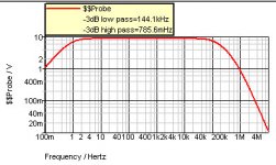
This buffer makes it possible to keep a high input resistor (R14) in the front, and because of the low capacitance load (like a lowpassfilter) we get a significant higer highfrequense roloff.
Because of the higinputimpedance (mainly R14) we can use much smaller inputcaps, here 4,7uF, (like in a highpassfilter) and have a -3db rolloff a little under 1 Hz.
This is the main cause to the wider bandwidth as I see it, and again I am shure that tere is much more to this.
In the simulation, the sourcepin at the inputbuffer have a dcpotentiale at 0,08V and the gate have -3,79V, this could be adjusted through R10 to obtain 0V at the buffers sourcepin. But I don´t think that this 0 is important, as long as it stays within say +- 2V, but a difference in voltage between the two complementary buffres sourcepins ar important to keep dc at the output near 0.
I dont think that a Voltage change at the buffers sourcepins will alter the bandwidth, but it can have some major influence at the symmetry of the singlended voltage swing when clipping.
As I understand the "Penultimate inputbuffer", it is the low input capacitance at 50 pF on the gate of ZVP3310, where IRFP140 has a 1700 pF inputcapacitance.
This buffer makes it possible to keep a high input resistor (R14) in the front, and because of the low capacitance load (like a lowpassfilter) we get a significant higer highfrequense roloff.
Because of the higinputimpedance (mainly R14) we can use much smaller inputcaps, here 4,7uF, (like in a highpassfilter) and have a -3db rolloff a little under 1 Hz.
This is the main cause to the wider bandwidth as I see it, and again I am shure that tere is much more to this.
In the simulation, the sourcepin at the inputbuffer have a dcpotentiale at 0,08V and the gate have -3,79V, this could be adjusted through R10 to obtain 0V at the buffers sourcepin. But I don´t think that this 0 is important, as long as it stays within say +- 2V, but a difference in voltage between the two complementary buffres sourcepins ar important to keep dc at the output near 0.
I dont think that a Voltage change at the buffers sourcepins will alter the bandwidth, but it can have some major influence at the symmetry of the singlended voltage swing when clipping.
Buffered x-soz
I'm glad to someone else taking up the x-soz challenge, Henrik. I hope you don't mind, but I've taken the liberty of modifying your circuit in an attempt to improve its performance further. The main change is to connect the input buffer to the diff pair 'tail' rather than to -ve. This operates it under conditions more like the Zen V4, reducing distortion and power dissipation. I've also substituted the ZVP3306 and I'm lead to beleive that the ZVP3310 may be even better due to its lower capacitance. I didn't have a model of the latter to hand which is why I didn't use it. I've changed the biasing a little to minimise distortion and reduced the current in the buffer. The latter change results in only a very small increase in distortion (approx 0.001%) and usefully reduces dissipation.
I hope this is useful and I would appreciate it very much if you would like to try it. I will do so too, but I don't have a SOZ available at the moment.
Ian.
Attachments
Ian
I actually hoped You would come back, more than welcome!
Wen I was drawing the first scematic, I realised that the Vds at the buffer was too high, generating too mush unlinearity or distortion (outputcharacteristica from datasheet), so I would like to make a suitable negative voltage refrence somehow, but I did not find it at first, so therefore I quickly tied the drain to -ve. I was looking for the wider bandwidth, and that I got in this first shut.
I do have somequestions to You:
At the node for the two tied sourcepins of the IRFP140´s You will se som voltage swing from the signal, not much, but it is there. The amplitude of this swing is in bal. mode 15mV and in unbal. mode 300mV.
1) When You tie the buffer drains to this node, woun´t You then get som feedback this way and thus having two feedbackloops?
2) If You get this feedback, will it matter at all?
3) Is there other benefits tieing the bufferdrains to the sourcepins of the IRFP140´s besides from getting a suitable negative voltage refrence?
4) As You can see in my scematic, I have used some zeners to make this negative voltage refrence, it works fine in the simulator, but could there be some hidden problems in this?
5) You changed the bias a little, and as far as I can se, you have mediated the voltage betwin the gate and the sourcepin at at the inputbuffer. Why will this better the distortion figurs?
The current through the buffer in my first scematic was too high, In Zen Var4 Nelson used 7mA, therefore I have increased R3 from 680E to 2.7K.
6) Any particular reason You have chosen R3=1K or 19mA current?
Your aproach to this is very usefull to me, I am learning a lot from this too, and I hope You will answer at least some of my questions.
I need to get the ZVP3310 from Digikey first, so it will take some time to do this.
Thancks for Your post.
Attachments
Tying buffers ro diff pair tail
Hi Henrik, good to see that you are questioning my suggestions rather than blindly accepting them. I do have some answers for you, hopefully useful. First off, why did I tie the buffers to the diff pair ‘tail’? Your guess is at least partly correct: the diff pair tail is a useful source of negative voltage at about the right voltage. However, there is another and perhaps better reason. Connecting the buffer in this way effectively operates it at almost constant Vds (due to the Vgs of the diff pair MOSFET). This might be regarded as a sort of cascode arrangement and has the usual advantages, namely reduced distortion in the buffer stage. Of course you can use the zeners as per your schematic but then you will not get the cascode effect. However, I’m sure they will work just fine.
Does tying the buffers to the tail result in another feedback loop? I don’t think so, at least not in the conventional sense. Any voltage at the diff pair tail is effectively the result of the buffer output (which will be much the same as the input signal) and is in phase with it. Other than the cascode action already mentioned, I don’t see any other form of feedback, undesirable or otherwise.
Regarding the biasing, this is the result of another almost inevitable compromise. The most important aspect here is arranging for the correct voltage at the drains of the output devices. Correct in this sense being a compromise between maximum output voltage swing and avoiding excessively low values of dynamic Vds due to signal excursion. The latter region of the output devices being less linear. I chose a value of bias that gave the least distortion at close to the maximum signal level.
Finally, on to the current through the input buffer device. In general, the higher the current, the lower the distortion. I started from your value and decreased the current until the distortion started to increase measurably. That said, this is a pretty low level effect and I am sure Nelson’s figure of 7mA would do just fine.
I hope this helps. I too am keen to learn more as a result of our collective exploration.
Ian.
Ian ,
for example I don't understand (or don't agree) that way to connect the buffer.
First I don't recognize a cascode operation,
second ,talkin' about phase ,the signal from the buffer goes to the source of the diff pair in phase, while if you connect a resistor
between the drain of the buffer and -V you will find at this point a
amplified signal wich will be inverted on the phase.
Notwithstanding this , I started to see clearly through the SuSy concept ,thanks even to our considerations and those of MR Pass.
Pretty soon I'll come back with a schematic for a comparison.
Stefano
Stephano
You may be right but I don't think so. Perhaps I confused the issue with my reference to cascode operation. All I meant was that the buffer device is being operated at a near constant Vds (like, but not the same as, a cascode) since the Vgs of the output device acts like an almost constant voltage source. This will also effectively conduct any signal across the buffer device so I don't think there is any issue with an out of phase signal appearing at the buffer drain.
Ian.
Ok , seems allright ...
Here is a feedback arrangiament around the differential pair.
The loop is actually not including the output stage.
Ian , Henrik
I play around with some resistor values , but you with your
simulating sistems could help find more appropriate ones.
Any way , I started with :
R12-R15 1.5k
R10-R11 1k
R13-R14 200k
May be good put some imput resistor to ground.
Stefano
Ian
Thaks a lot for Your answers.
I try real hard to go deeper into the understanding of this buffer, it is hard to beleve, that scuch little peaces of plastic with only 3 legs can be so hard to understand, amaizing.
I got your point on tieing the the buffer sources to the tail, but I still can´t make room in my imagination to see if it works or not, and that is becauce I need som more bacic understanding of how little plastic-things works.
So I wil go on to get som literature on the subject. If You have some recomadations, please let me know.
Stefano
I know the benefits of using cascode, so it is obvius to me that this buffer is not, but there coud be some common operating conditions, as I read Nelsons article Zen Var4 I got that feeling, but since I dot understand his word fully, it is hard for me to get an opinion on this. You don´t beleve in this coupleing bufferscources to the diff. tail, and I am shure You have Your resons, but I cant at the moment see wether it works or not, sorry.
In Your scematic, You omited the the feedback at the output, I regard these as the fundamental diff. pair, around wich we shoud make the x-feedback, so taking them out is in my humble opinion to leave the X behind and make some local feedback at the inputs. Don´t the X-feedback need some "tails" to work through? In the Aleph-X it was the input diff. pair tail.
I am up to do this X-SOZ, but it might take some time.
But to day I order som parts at Digikey, but how long it takes before I get these parts is hard to say.
Keep up the good work!
I have some studing to do first, I will come back later.
Stephano
I admit to being a little bewildered at what you are trying to achieve with your circuit suggestion. Why place feedback round the buffer stage, it is already quite linear and the circuit does not require any output from the drain. I agree with Henrik that the most non-linear devices are the diff pair and this is where the feedback really counts. Your alternative is not an X either, so any advantage from this mode of working will be missing from your suggestion.
Ian.
Ian
My frustration not understandinig it all yesterday was leading my post, an You did answer some of my questions to which I didn´t make any comments.
Your changes to my first circiut, except the main issue about tying the buffers drains to the tail at the output pair, I can agree with.
You changed the bias point for the diff. pair by changing R10 (in mys scematic) from 360K to 680K, thus giving a more symmetrical waveform when approching klipping. Nice, I have changed that too in my scemtic!
You also changed the current trough the buffer, and even if it only decreases the distortion very little, we take that too as long as we keep Vds around -4V, conciderd and done.
The size of the inputcap (22uF) in Your scematic gives som -3 db lowfrequince rolloff at 0,17 Hz, against my 0,79 Hz with 4.7uF.
I think this difference is more a private matter, I will prefer to use mor money on better quality caps at lower value than the other way around.
I can´t give you my opinion on where to put the drains of the buffer, You may get it if or when I get a better understanding of little peaces of plastic withe three legs.
- Home
- Amplifiers
- Pass Labs
- x soz