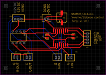
Hi all,
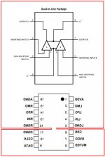
I am designing a Volume/Balance controller based on the WM8816 chip. I know there are millions of ready to use designs, with this or similar chips, in this forum (ie https://www.diyaudio.com/forums/analog-line-level/325268-balanced-volume-controller-line-stage.html, https://www.diyaudio.com/forums/ana...-6-input-selector-mdac-attenuator-ir-etc.html or https://www.diyaudio.com/forums/ana...eamp-arduino-remote-volume-input-control.html). But I'm aiming at the simplest possible implementation based on the Typical Application (Figure 5) in the WM8816 datasheet, because I just need SE-SE.
I'm looking for comments and ideas to improve both the design and my (lack of) EasyEDA skills, since this is my first ever PCB "design". So please bear with me.
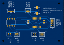
Thank you so much
I am designing a Volume/Balance controller based on the WM8816 chip. I know there are millions of ready to use designs, with this or similar chips, in this forum (ie https://www.diyaudio.com/forums/analog-line-level/325268-balanced-volume-controller-line-stage.html, https://www.diyaudio.com/forums/ana...-6-input-selector-mdac-attenuator-ir-etc.html or https://www.diyaudio.com/forums/ana...eamp-arduino-remote-volume-input-control.html). But I'm aiming at the simplest possible implementation based on the Typical Application (Figure 5) in the WM8816 datasheet, because I just need SE-SE.
I'm looking for comments and ideas to improve both the design and my (lack of) EasyEDA skills, since this is my first ever PCB "design". So please bear with me.

Thank you so much
Attachments
Using wide short traces from power and ground pins to ceramic decoupling caps is customary to provide less stray inductance on those routes.
Ground-planes are normally used, separate ones for digital and analog joined at single star-grounding point.
Ground-planes are normally used, separate ones for digital and analog joined at single star-grounding point.
Using wide short traces from power and ground pins to ceramic decoupling caps is customary to provide less stray inductance on those routes.
Ground-planes are normally used, separate ones for digital and analog joined at single star-grounding point.
Hi
I thought about it yesterday and even tried to add two ground planes, but being my first PCB attempt I couldn’t find the space. Maybe if I put the WM chip on the bottom side I can probably reposition the caps closer to the chip pins. Will try later this weekend.
Thank you!
OK, tried my best.
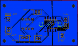
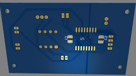
I moved the WM8816 chip to the bottom layer and repositioned all elements. I think caps are much closer to the pins now.
Also created two ground planes, but I was not able to join DGND and AGND planes, auto-router was destroying the join trace all the times. So I created a 0R resistor to function as a GSTAR. It's possibly the worst of the idea
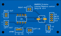
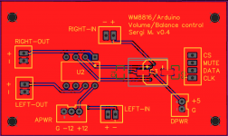
Here's the updated files:
Photo view:
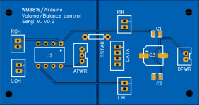
Wiring top view:
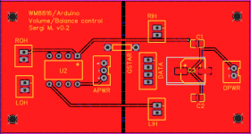
Wiring bottom view:
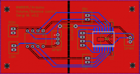
Thank you again for the help.
I moved the WM8816 chip to the bottom layer and repositioned all elements. I think caps are much closer to the pins now.
Also created two ground planes, but I was not able to join DGND and AGND planes, auto-router was destroying the join trace all the times. So I created a 0R resistor to function as a GSTAR. It's possibly the worst of the idea

Here's the updated files:
Photo view:

Wiring top view:

Wiring bottom view:

Thank you again for the help.
Attachments
Is using a 0R resistor (or short piece of wire) to join digital and analog ground planes a bad thing?
Is using a 0R resistor (or short piece of wire) to join digital and analog ground planes a bad thing?
Using a 0R resistor will work, otherwise try to look into using a "Net tie" instead.
I am more concerned by how you split the groundplane tbh. This makes no sense whatsoever as shown. You want the analog groundplane under the WM8816 analog section, too. I think you'd best rotate the chip by 180°, so that you get a chance of giving the digital stuff a little corner of its own.
Also, the connection from LMO/RMO to the opamp's inverting inputs should be as short as possible to avoid undue capacitive coupling; perhaps even consider sparing out the groundplane underneath.
Splitting the groundplane under the chip used to be a common recommendation for mixed-signal ICs (like DACs) in the 2000s. Eventually people found that they could actually get better performance out of a non-split groundplane after all, but for something like a WM8816 this should work perfectly fine.
If you have a spot for a 0R resistor already, I would reserve another for a ceramic capacitor next to it.
You only need to discriminate in the layout between analog and digital ground, in the schematic they can be the same signal - then all you have to do is provide a narrow neck in the ground-plane as the join point.
Remember the whole point is to keep digital current flows from going near any analog routing. Digital currents are very noisy even if a few mA because they slew in a few nanoseconds.
Remember the whole point is to keep digital current flows from going near any analog routing. Digital currents are very noisy even if a few mA because they slew in a few nanoseconds.
Hi everyone, and thank you again for hand-holding me through the learning process.
OK, I drew what I understand from your words in the attached image.
The WM8816 chip was already in the bottom layer in previous design, because I think it makes positioning the caps a bit easier, so it's actually rotated to make the analog side closer to the opamp. I just drew the ground layer with the small join just in the middle of the chip, but the chip is on the other side, so should I create another ground layer in the bottom side?
Thank you again, sorry for the stupid questions
Using a 0R resistor will work, otherwise try to look into using a "Net tie" instead.
You only need to discriminate in the layout between analog and digital ground, in the schematic they can be the same signal - then all you have to do is provide a narrow neck in the ground-plane as the join point.
I am more concerned by how you split the groundplane tbh. This makes no sense whatsoever as shown. You want the analog groundplane under the WM8816 analog section, too. I think you'd best rotate the chip by 180°, so that you get a chance of giving the digital stuff a little corner of its own.
OK, I drew what I understand from your words in the attached image.
The WM8816 chip was already in the bottom layer in previous design, because I think it makes positioning the caps a bit easier, so it's actually rotated to make the analog side closer to the opamp. I just drew the ground layer with the small join just in the middle of the chip, but the chip is on the other side, so should I create another ground layer in the bottom side?
So the alternative would be to have a digital ground in bottom layer (chip layer) and the analog ground in the top layer (opamp)?Splitting the groundplane under the chip used to be a common recommendation for mixed-signal ICs (like DACs) in the 2000s. Eventually people found that they could actually get better performance out of a non-split groundplane after all, but for something like a WM8816 this should work perfectly fine.
Noted, thank youRemember the whole point is to keep digital current flows from going near any analog routing. Digital currents are very noisy even if a few mA because they slew in a few nanoseconds.
I will make sure to position the opamp closer to the chip, moving the data header to the other side.Also, the connection from LMO/RMO to the opamp's inverting inputs should be as short as possible to avoid undue capacitive coupling; perhaps even consider sparing out the groundplane underneath.
Do you mean the join of the planes should also have a capacitor?If you have a spot for a 0R resistor already, I would reserve another for a ceramic capacitor next to it.
Thank you again, sorry for the stupid questions
Attachments
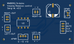
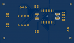
OK I repositioned everything, trying to take into account comments above.
Top layer includes the opamp chip, all header and the big(er) cap, and a copper layer.
Bottom layer includes the WM8816 chip and the two smaller caps, plus a copper layer with a H shape trying to make a split between digital and analog areas of the chip. Chip was turned 180 degrees to face the analog side closer to the opamp, and data header is now on the other side as well.
Here's the outcome design. Do you guys see any big issue?
Thank you so much again
Attachments
Last edited:
OK, changed a little more the ground layers, caps package and repositioned slightly.
Still interested in feedback and suggestions, otherwise I think this v0.5 will be sent to fabrication soon-ish.
Thank you so much
Still interested in feedback and suggestions, otherwise I think this v0.5 will be sent to fabrication soon-ish.
Thank you so much
Attachments
- Home
- Source & Line
- Analog Line Level
- WM8816 Volume/Balance Controller: Request for comments
