Again throwing some components into the simulator...
O.K. using your last circuit http://www.diyaudio.com/forums/attachment.php?s=&postid=720447&stamp=1126311987
It can easily modified in order to work. Get rid of C1 and C3, connect the anode of D1 to the collector of U3 and the cathode of D2 to the collector of U4, increase R4 and R8 to 1/10 of R5 and R6 (38,3k). If you are not biasing U3 and U4 in any way there will nothing happens. Decrease R1 and R2 to about 220 Ohms (not critical). You'll get about 0.72V across R1 and R2. This is all simple math not more than a voltage divider and adding/substracting Vbe after that. As I've said before, BUILD your circuits not (just)simulate them. You will have a steep learning curve. If you know what you're doing you can simulate it. Calculate your circuits do not using a try and error method. If you feed nonsens into a simulator it will output nonsense! Later on in your job you'll get in serious trouble if you design just by throwing components in your sim. No one will have appreciation for discussions of nonworking circuits.
this is not my last circuit.
THIS IS MY LAST CIRCUIt:
http://www.diyaudio.com/forums/attachment.php?s=&postid=721943&stamp=1126550008
THIS IS MY LAST CIRCUIt:
http://www.diyaudio.com/forums/attachment.php?s=&postid=721943&stamp=1126550008
Well, here we go again.
For starters, it would be nice if you learned that Si BJTs require 0.6V or so between B and E to be in active mode given non-zero and proper polarity voltage between C and E. So far you have demonstrated a nearly complete lack of understanding of basic biassing, and worse, of Ohms, Kirchoff and Joule's laws, all basic stuff.
All I can say is, good luck with your latest curcuit.
I have better things to do with my time than waste any more here. I think I have shown more patience than most, but still, I can only give up.
the only problem with the circuit is the power dissipation at the output resistors. Bias is perfect, no way it can be wrong.
Hi Ashade,
don't worry about meeting up with a steep learning curve. It will never happen to you.
Bocka,
give up.
don't worry about meeting up with a steep learning curve. It will never happen to you.
Bocka,
give up.
1) You are joking with us
2) You are unwilling to learn the basics
3) You are unable to learn the basics
ashade,
Point 2 and 3, you are unwilling and unable to learn the basics. You are unwilling to build your circuits as well as trying to learn from some people of us, who building circuits for years or better sait 10th of years with sometimes more than 1000 components and much more complexity than a simple amplifier. We're designing PCBs where analog stages are located with digital components in direct proximity, running with some 10th or more MHz. No simulator shows you the influence of crosstalk in such an environment. None of us is perfect and we're all doing a lot of silly mistakes, but we learn what we're doing wrong.
You do not look into datasheets. You do not learn that the forward voltage of a (junction) Si diode is about 0.6 to 0.7 volts. In addition for more than 99% the first rules of arithmetic are enough for an elementary design. You do not calculate anything. You are unable to learn that two (identical) discrete transistors behave not the same. You have never mentioned that for the same collector current Vbe drops about with 2mV/K for each kelvin increasing. You design your circuits from scratch instead of using a functional design and modify it carefully, although your experience is zero.
Like ilimzn I'll leave this thread too
You do not learn that the forward voltage of a (junction) Si diode is about 0.6 to 0.7 volts.
So tell me which transistor is wrong biased.
ashade said:
So tell me which transistor is wrong biased.
Pretty much everyone, with the possible exception of U3.
What is, for example the voltage at the base of U4? Answer: 0.6 volts higher than the base of U1.
What is the voltage at the base of U1? Answer: 0.6 volts higher than the voltage at the emitter of U1.
What is the voltage at the emitter of U1? Answer: That depends on the current through R11.
What is the current through R11? Answer that depends on the voltage at the emitter of U3.
What is the voltage at the emitter of U2? Answer: 0.6 volts higher than the voltaga at the base of U2.
What is the voltage at the base of U2? Answer: that depends on the current through R4.
What is the current through R4? Answer: that depends on the voltage at the base of U2...
Basically there is nothing that fixes the operating points of any of the transistors. The current through U2 depends heavily on the exact value of hFE/beta, which varies a great deal. Same thing with U1, U4 and U1.
Rune
one thing is saying that the bias of the transistors are highly dependent on each other. This is true. Another thing is saying the bias is wrong. It's not. Everything is active. Take a good look:Basically there is nothing that fixes the operating points of any of the transistors. The current through U2 depends heavily on the exact value of hFE/beta, which varies a great deal. Same thing with U1, U4 and U1.
U3 -> emitter follower stage using high hfe pnp bjt. Hence, current through voltage source (including inner resistence R9) is near zero (about 200nA against spice simulation). So, the DC voltage at its base is about 200-250uV. Assuming a drop of 0.65V (looking on datasheet of BC559C), potential at emitter of U3 is about 0.65V, which is also the Vbe value for Q2 gain stage.
Q2 -> Common emitter config. I tryied to bias with Ic = 10mA, but it's not good since it exponentially depends on Vbe value. Thus about 0.01 changes on Vbe will dramatically change Ic bias. I assume this is not a good biasing, but still works. My idea is to bias so that potential at q2 collector is 8.1V, letting a maximum swing of 1.2V .. 15V (less than 0.65 it begins saturation).
U4 -> another emitter follower. Bad choice since this bjt has very low hfe. I'm gonna take R5 off cause it's not needed and change this bjt by another MPSA18.
Output stage-> I tryied to bias Ic = 3A for the ouput transistors, but also too hard because it depends on very unstable parameters. Also, 3A for any resistor will mean lots of power dissipation, hence this is not a good output stage also.
I'm trying to make an amp as simple as possible, with at max 6bjts just to build and try to learn something. But every amp I see has lots of bjs and I can't make a simple one to work because it has lots of limitations, like biasing, output offset, power dissipation, etc...
I know how to fix the last schematic, but I think I will have to put at least 4 more bjts, make feedback, current sources, etc, which will rise the complexity of the circuit. However, I promisse I'll study hard in my books and the next circuit I post here will not be so stupid the the last ones.
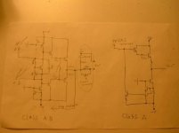
These are somewhat legitamate output topologies. Current sources can be made different ways, using diodes, ect., but it gives you the idea of proper bias. Of course modifications can be made, but bias cannot be beta dependent for stable operation. If you design a bias around the beta variable, bias will vary depending on the specific transistor and temperature.; I mean individual device, because every transistor is unique and not identical even if it is the same number. Look at the gain (beta) curve of any transisor data sheet and you will notice different curves for different temperatures. This temperature can vary as fast as the signal peaks....vary fast instantanious change. If the bias is beta or temp dependent, it can change that fast. You don't want your BIAS to change much.
Zobel network is for RF rejection. Basic AC electronic theory should explain why this is.
The Vbe multiplier should be mounted with the outputs to track temperature because Vbe turn-on of the output devices depend on temperature. This creates a thermal feedback system to keep bias the same regardless of temp IOW, making the output bias NOT temperature dependent. The pot is to adjust output bias.
Attachments
- Status
- Not open for further replies.
- Home
- Amplifiers
- Solid State
- Why always differential stages?