Hi Qsa,
The Nmos series was not designed to run on rails higher the 85v and even then will run quite hot. I imagine at 100v it would run too hot to be practical.
The series was designed for domestic use only so for PA use I suggest the Actrk series which is more efficient because it can swing rail to rail.
Sorry I can't support more development in this amp, I simply do not have the time, but it's good to see that people like yourself are making changes and improving it.
Cheers
Q
So I guess this is on-topic... There is at least one way to construct a completely symmetrical quasi-complementary amplifier: Couple drive to the output devices via opto-isolators, using floating power supplies on the photodiode side to power each base/gate drive circuit. I built a test circuit several years ago, using a couple of wall-wart PSUs and video op-amps to drive power MOSFET gates. It had a linearity problem that stacked up with isolator and MOSFET characteristics, but the concept might have legs.
I post my result here, It is quasi IRFZ44, 70V-class,500W tracking rail. But only simulation result by now. I am going to realize it later.
http://www.diyaudio.com/forums/ever...eally-i-post-some-proof-here.html#post2203189
http://www.diyaudio.com/forums/ever...eally-i-post-some-proof-here.html#post2203189
Last edited:
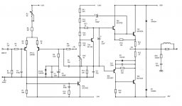
Help.
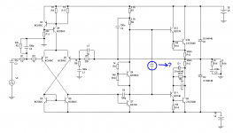
Somebody please tell me what the importance of the diode and the resistor inside the pointed area is.
Thanks.
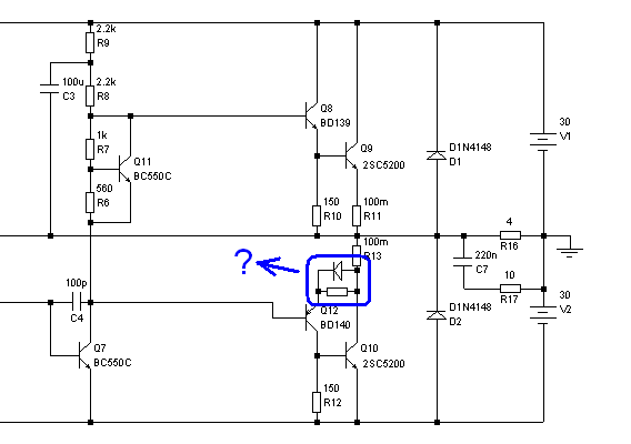
Somebody please tell me what the importance of the diode and the resistor inside the pointed area is.
Thanks.
Q8 (the driver) sees as it's load :-
R10//Q9base
Q9base is just about equivalent to a diode//capacitance.
The effective load on Q8 is thus R//D//C
For good equivalency the complementary driver Q12 needs to see the same load on it's emitter. That R//D + R13 is an attempt to mimic the Q8 load, but the C has been omitted. The R is also in the wrong place. It is not in series with 0r1 (R13) The D//C only are in series with 0r1
To correct the partial schematic.
Remove the unlabeled resistor and replace it with a capacitor.
Now add a resistor (150r) from Q12 collector to the output (same connection as R10)
The three components now mimic the Q8 load. The difficult bit is finding the C value and picking a diode that is roughly similar to the "be" junction of Q9.
Both resistors are already defined in the upper half and the lower half matches them.
You still need R12 to define the current through the driver Q12.
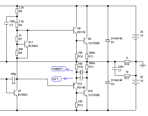
Thanks AndrewT.
I think the diagram below is what you suggest.
The simulator shows no change in performance Except bias decrease. That can be fixed and with 100mA it's as it was before.
Any suggestions for the diode and the capacitor? Do the shown things seem good??
Thanks.
I think the diagram below is what you suggest.
The simulator shows no change in performance Except bias decrease. That can be fixed and with 100mA it's as it was before.
Any suggestions for the diode and the capacitor? Do the shown things seem good??
Thanks.
Last edited:
You had it right the first time Shaan, you just needed to make both resistors around Q12 150 ohm. Andrew, the resistor and diode should be connected to the collector of Q10 not the output. Baxandall is quite clear about this 🙂
I don't know about Baxendall but i'm in 100% agreement on this. If the network is connected to the output then there is nothing to stop Q10 from attempting to conduct horrendous amounts of current. I learn't by this mistake by blowing about £25 of TO3s 😱 With the network connected to the collector of Q10 so R13 is between it & the output there is local feedback which will prevent silly things happening 🙂the resistor and diode should be connected to the collector of Q10 not the output. Baxandall is quite clear about this 🙂
oops
really big oops.
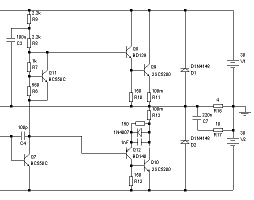
Sorry to all those misled by my suggested placement for the 150r.
150r is back where it was, keeping the extra cap and the resistor in parallel with the diode.
really big oops.
Sorry to all those misled by my suggested placement for the 150r.
150r is back where it was, keeping the extra cap and the resistor in parallel with the diode.
Don't worry no problemo. I haven't yet soldered the three components to the board. But now I will.
Almost, but R10 should connect to Q9 emitter. that puts everything in series with the 0r1 on both sides
The diode is Shaw's addition.
The resistor is Baxandall's addition.
The capacitor is JLH's addition.
The diode is Shaw's addition.
The resistor is Baxandall's addition.
The capacitor is JLH's addition.
Almost, but R10 should connect to Q9 emitter. that puts everything in series with the 0r1 on both sides
Hey that's a good idea. I hope i'll be able to do it in the board.
No it's not a prob at all! And also the power stage looks much more "balanced" with R10 between emitters of Q8 and Q9! 🙂
that's exactly why the JLH addition exists. to allow the two drivers to see near enough an identical load..........the power stage looks much more "balanced" with R10 between emitters of Q8 and Q9! 🙂
JLH suggests C=20pF and D=is920 (or is820, I can't read it clearly) for Re=0r22, R=R10=R12=100r and 2n3442 outputs.
which sounds better a quasicomplementary amp or a complementary amp as i going to make a amp in the range of 150 to 200W rms I was just thinking which topology to use .................
Comments Plz
QC measure worse than complementary , but the distorsion
can be more regular, in that the harmonics deacrease with frequency
until the feedback vs frequency ratio become inneficient..
That said, i don t think that a (quasi !) monotonic deacrease
of a THD ratio of 0.1% is a better result than a less
monotonic figure with a THD of 0.02%..
There s surely far more influence for the tonal result
in the amp/load matching...
- Home
- Amplifiers
- Solid State
- Which is Beter Quasi Or Non Quasi