Some pics of a humble-2hours-non-definitive-work with the sinchronous recloker did yesterday and from wich I am truly pleased as sonic results.
It consists in 4 FF each one with its PS (battery) .Each FF recloks in turn the DATA+ DATA- BCK and WS:
The first pics shows a panoramic of the "modular" SR with the batteries
It consists in 4 FF each one with its PS (battery) .Each FF recloks in turn the DATA+ DATA- BCK and WS:
The first pics shows a panoramic of the "modular" SR with the batteries
Attachments
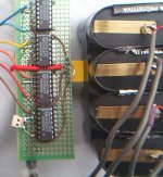

the third shows the back of the board with some cheap cap and ferrite beads for decouplin 🙂
I would make a definitive board of this project: Tent clock,sinchronous reclocker , 2 TDA1543 in balanced mode , D1 output stages . But first I have to find some smd single package FF and XOR and see if I am able to soldering that tiny parts .
I would make a definitive board of this project: Tent clock,sinchronous reclocker , 2 TDA1543 in balanced mode , D1 output stages . But first I have to find some smd single package FF and XOR and see if I am able to soldering that tiny parts .
Attachments

Bernhard said:Stefano,
very nice but what about a schematic, or can you explain me ?
Bernhard,
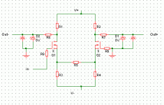
This is a Sinchronous Reclocker or sinchronizer. It use only one flip flop par line. The lines are 4 : BCK , WS , Data+ and Data- : the I2S plus an additional inverted data that creates the balanced DAC.
The trick (?) was to use separated flip flop(and Chip) for each line, for the control of the ground bounces and induced jitter .
Each flip flop has its PS -batteries for the case - and it is controlled sichronously by the master clock of the CD player(at the freq of the CD player) . The clock has to be placed near the sinchronizer and the dacs ,and from there , feeded back to the CDP .
Have no measurements , but the improvement is sonically MORE THAN EVIDENT if compared to a single chip containing more than one flip flop and WITH one PS.
edit -
set up is :
saa7310
Tentlabs XO
XOR buffers
shielded cables
tda1543 in balanced mode
Passlabs D1 I/V stages
search the forum for more info
😎
Bernhard said:What I like to know is how you connect the flipflops.
Set reset clock data...
set and reset at +VCC ,
data is where the line enters the FF
Q is were it goes out
Qneg is a complement and not used in this case.
The clocks all together (4 clocks)
Since the package contains 2 flip flops , put to GROUND the input and clock pins , and at VCC set and reset of the second flip flop.
(suggested by Bricolo and works fine).
Bricolo said:The only single gate packages are the very small picogates 🙁
Sig..

lets organize a board , professional made , with the pico gates already soldered , multiple use .

The only single gate packages are the very small picogates
lets build discrete inverters.
stefanobilliani said:
Qneg is a complement and not used in this case.
Ok, thanks, just a quick thought :
Why not use the complement for the inverted data line ?
Bernhard said:
Ok, thanks, just a quick thought :
Why not use the complement for the inverted data line ?
Yes, works fine.
differential pairs, driven with a higher than 5V PS, high limited to +5V with zehner, can be used as buffer or inverter without any time offset between inverted and noninverted signal.
do we really need flip flops?
Isn´t it inacceptable in an aesthetic point of view to use ICs and have loads of pins unsued? I would prefer to avoid ICs not really needed.
In my subjective view there are 2 proper ways: discrete, or DSP.
do we really need flip flops?
Isn´t it inacceptable in an aesthetic point of view to use ICs and have loads of pins unsued? I would prefer to avoid ICs not really needed.
In my subjective view there are 2 proper ways: discrete, or DSP.
till said:
Isn´t it inacceptable in an aesthetic point of view to use ICs and have loads of pins unsued? I would prefer to avoid ICs not really needed.
Yes it is unaceptable , let's use pico gates single packages!
let's use pico gates single packages!
a) do they provide syncronous buffered and inverted signal like differential pairs?
b) as there is a lot rumor about common mode rejection and poluted power supplys with TTLs, did you think about a class a inverter / buffer?
think a small high speed BZLS, output forced not to go over 5V.
c) what about some kind of philosophical coherence in the chain: Pass style signal conditioner - balanced DACs - D1 - BZLS - SOZ
Try it. But I don't think that discrete can be fast enough
About the TTL noise. You're right. But nobody uses TTL anymore 😉
About the TTL noise. You're right. But nobody uses TTL anymore 😉
- Status
- Not open for further replies.
- Home
- Source & Line
- Digital Source
- Where does jitter come from?