I'm building a PCM1794 DAC, planing to have line-out, headphone amp, maybe fully-differential low-pass filter for balanced output, with line-out it's just datasheet low-pass filter, but headphone amp I'm planing to use TPA6120, which requires differential input, would it be a good idea to split the signal after I/V stage? if current output isn't an issue(using opa1612), one goes to opa1612 as in datasheet, one goes to TPA6120 without buffer?
what's normal way to handle multiple output?
thank you all


what's normal way to handle multiple output?
thank you all
I think that should work well, tapping the signal off from both current-to-voltage converters, that is. The reconstruction filter for the headphone path is then only first order, but considering the huge slew rate of the headphone amplifier, the switching residues are not likely to cause trouble.
Do you intend to use fully digital volume control for the headphone?
Do you intend to use fully digital volume control for the headphone?
Thank you for the answer. I'll go fully digital volume control with the headphone, bcs If I put volume control, wouldn't do it on the differential part, so it will be after the single ended low pass filter, then potentiometer, then TPA. Quality potentiometer is pretty pricey and it will make the signal chain a bit longer.
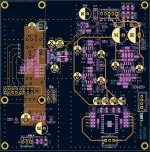
any suggestion on how to handle the ground? I'm planning to use 4 layer board for this project.
any suggestion on how to handle the ground? I'm planning to use 4 layer board for this project.
I use the inner layers as ground planes and the external ones for signal and supply traces. Sometimes an inner layer has to be used for a crossing, interrupting the ground plane. I try to keep such traces short and often add vias to ground fill on the top or bottom to ensure that return currents don't need to take a big detour. No idea if it is optimal in any sense, but it works reasonably well.

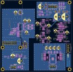
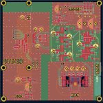
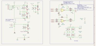
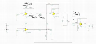
After a bit of study and dug thru datasheets, this is my progress so far. I try to protect the digital line as much as I can, and keep analog to one side. I dug out TPA6120's input ground plane as EVM board showed, it's a CFB amp, which needs a bit care for it's high slew rate. For opa1611 I/V, differential, just the usual layout. I'm using taobao Amanero board and plan to modify the USB power part, I it can use my board as power source.
are there any fault or anything I can do to improve this?

are there any fault or anything I can do to improve this?
Attachments

You have to look out for the load on the I/V converters. Right now it is at 680 Ohms and you plan to take an output there, probably to another balanced to single ended circuit.
Thank you so much, you've always been helpful.Nothing I can think of, it looks good to me.
Ok, so a load of 400 Ohms. Bit low perhaps?
Closer to 210 ohm for the negative current-to-voltage converter, I think. It is a bit low, but not low enough to drive the op-amp close to current limiting, I suppose. These DAC reconstruction filters are always low-ohmic to keep the noise voltages low.
Calculated more accurately, for frequencies well below cut-off:
Headphone amplifier negative input: 1 kohm to 1/2 of the voltage on the positive input -> 3/2 of the negative input's signal voltage acrods the 1 kohm, so effectively 2/3 kohm load
Line differential amplifier negative input: 680 ohm to 330/(680 + 330) times the positive input voltage -> effectively 680 ohm/(1 + 330/(330 + 680)) ~= 512.5373134 ohm
Current-to-voltage converter feedback: 820 ohm to virtual ground -> 820 ohm load
All of it in parallel: ~ 214.1057283 ohm
There is apparently 2.2 V RMS coming out of the differential amplifier for the line output. Calculated back, that's 2.26666... V RMS at each of its inputs/each current-to-voltage converter output.
Signal current coming out of the current-to-voltage converter op-amps: 2.2666... V/214.1057283 ohm ~= 10.58666989 mA RMS, 14.97181213 mA peak.
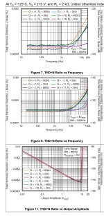
An OPA1611 can typically deliver more than 40 mA peak. The distortion graphs are all at 7.071 mA peak or less, though.
Summarizing, it is a bit low, but not low enough to get close to current limiting.
Headphone amplifier negative input: 1 kohm to 1/2 of the voltage on the positive input -> 3/2 of the negative input's signal voltage acrods the 1 kohm, so effectively 2/3 kohm load
Line differential amplifier negative input: 680 ohm to 330/(680 + 330) times the positive input voltage -> effectively 680 ohm/(1 + 330/(330 + 680)) ~= 512.5373134 ohm
Current-to-voltage converter feedback: 820 ohm to virtual ground -> 820 ohm load
All of it in parallel: ~ 214.1057283 ohm
There is apparently 2.2 V RMS coming out of the differential amplifier for the line output. Calculated back, that's 2.26666... V RMS at each of its inputs/each current-to-voltage converter output.
Signal current coming out of the current-to-voltage converter op-amps: 2.2666... V/214.1057283 ohm ~= 10.58666989 mA RMS, 14.97181213 mA peak.
An OPA1611 can typically deliver more than 40 mA peak. The distortion graphs are all at 7.071 mA peak or less, though.
Summarizing, it is a bit low, but not low enough to get close to current limiting.
Last edited:
Don't know how to calculate it, let me try, DAC will drain -2.6~-10mA, load is (820ohm I/V// 2k tpa6120// 1k low-pass) =~370ohm?Ok, so a load of 400 Ohms. Bit low perhaps?
so current is about 25mA? OPA1612 is capable of delivering but indeed on heavy side, No THD data for such load on TI's datasheet.
Attachments
I think all calculations on this thread are wrong. Mine are wrong because I forgot the -6.2 mA centre current, as you pointed out.
I put it in simulation.
IG center point -6.2mA, amplitude 3.9mA
U1 Vout =-8.28 , U1 sourcing 28mA
Load is about 295ohm.
indeed PCM1794 itself is heavy load, doable bit heavy.
If I go for I/V=> Buffer => Differential to Single
do I have to use opa1612?
So the circuit can maintain it's low noise 1.1nV performance.
if one stage I have to cheap out and use LME49720, which position is more suitable for it since it has 2.7nV as I remembered.
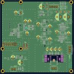
Attachments
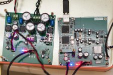
PCM1794+opa1612 I/V stage and opa1612 LPF, with TPA6120 headphone amp.
USB to I2S is Chinese clone amanero.
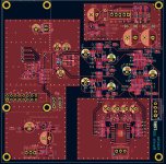
Finally finished. what a journey, especially try to hand solder 0402. In the end I added buffer between I/V stage and LPF, and branches to LPF, TPA6120 from buffer, it runs a bit hot, but total power draw is in spec. on signal path I use C0G 1% cap, 0.1% thin film resistor, C0G 47nF for decoupling. all the al electrolytic caps on DAC board are Panasonic FR series, the specs are just too beautiful.
Few quick notes for people try to make similar circuit.
PCM1794's digital switching noise is differential, so with TI's recommendation, I/V => TPA6120 even with 0.1% resistors try to gain more CMRR, you simply add the noise up, about 35mV on I/V stage, and 70mV on TPA6120 output, but it's in 1Mhz range. TI's recommendation is for budget design, better way is attached TPA6120 after LPF, where the digital switching noise is in 0.xmV.
TPA6120 runs pretty hot, idle 30mA, with +-15V, it will heat up PCB even with recommended layout.
The circuit is very quiet, if your design is budget sensitive, after I/V stage you don't need to use opa1612, won't make any differences noise performance.
Modify clone Amanero's power will improve sound quality a lot, I simply cut the 5Vbus, remove L1 and connect 5Vdc there. Gnd on the btm ground plane.
Overall it has good lows, fullness of instrument sound, clarity, very much like sound in expensive Cinema. But.... the soundstage is tight and something is off, really hard to tell, it's not very musical, and don't sound right in headphone. and you can sound silent pop when switching songs that's from the Chinese clone Amanero.
I think that might be from Chinese Clone, so, don't buy cheap chinese clone. my dac design and PCB should be fine.
my next step might be try different I2S interface,
or with isolator. I can't measure precious noise once USB plugs in,
somehow there's ground loop, PC power leakage, and it will show like 2mV ripple on every signal/power.
USB to I2S is Chinese clone amanero.
Finally finished. what a journey, especially try to hand solder 0402. In the end I added buffer between I/V stage and LPF, and branches to LPF, TPA6120 from buffer, it runs a bit hot, but total power draw is in spec. on signal path I use C0G 1% cap, 0.1% thin film resistor, C0G 47nF for decoupling. all the al electrolytic caps on DAC board are Panasonic FR series, the specs are just too beautiful.
Few quick notes for people try to make similar circuit.
PCM1794's digital switching noise is differential, so with TI's recommendation, I/V => TPA6120 even with 0.1% resistors try to gain more CMRR, you simply add the noise up, about 35mV on I/V stage, and 70mV on TPA6120 output, but it's in 1Mhz range. TI's recommendation is for budget design, better way is attached TPA6120 after LPF, where the digital switching noise is in 0.xmV.
TPA6120 runs pretty hot, idle 30mA, with +-15V, it will heat up PCB even with recommended layout.
The circuit is very quiet, if your design is budget sensitive, after I/V stage you don't need to use opa1612, won't make any differences noise performance.
Modify clone Amanero's power will improve sound quality a lot, I simply cut the 5Vbus, remove L1 and connect 5Vdc there. Gnd on the btm ground plane.
Overall it has good lows, fullness of instrument sound, clarity, very much like sound in expensive Cinema. But.... the soundstage is tight and something is off, really hard to tell, it's not very musical, and don't sound right in headphone. and you can sound silent pop when switching songs that's from the Chinese clone Amanero.
I think that might be from Chinese Clone, so, don't buy cheap chinese clone. my dac design and PCB should be fine.
my next step might be try different I2S interface,
or with isolator. I can't measure precious noise once USB plugs in,
somehow there's ground loop, PC power leakage, and it will show like 2mV ripple on every signal/power.
Attachments
Might be Chinese clone amanero attenuate high frequency.
After measurement,
LPF output 200hz 1Vrms,
6.4khz 560mVrms,
12.8khz 410mVrms
Headphone amp the same.
Measure from I/v stage output,
I+,I- 200hz 560mV, correct,
6.4khz 310mV, big nope
All the component on I/V stage, 820R // 2200p,
I measured before soldering, so, shouldn't be the problem.
It seems the problem should be that Chinese clone Amanero.
Those values deviate 0.5 dB...0.7 dB from the treble loss you would get by applying 50 us/15 us de-emphasis to a recording without pre-emphasis. The ideal values would be 1 V, 520.993 mV, 378.83 mV and 560 mV, 291.756 mV.
Thank you MarcelvdG, sorry I didn't make it clear.
I test it comparing to on-board sound card, with single strength around 1Vrms, at 200hz, 6.4khz,12.8hz.
On board sound card has flat frequency response.
Ideal should be 1Vrms across all frequency on my dac.
I test it comparing to on-board sound card, with single strength around 1Vrms, at 200hz, 6.4khz,12.8hz.
On board sound card has flat frequency response.
Ideal should be 1Vrms across all frequency on my dac.
Apparently I didn't make clear what I meant. If your USB interface or your DAC would have a built-in de-emphasis filter and if it would unintendedly be activated, that would cause almost precisely the errors that you measured.
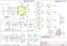
In fact, looking at the schematic in post #16, your DAC has a de-emphasis filter. Is jumper DE1 or DEM_JP set properly?
In fact, looking at the schematic in post #16, your DAC has a de-emphasis filter. Is jumper DE1 or DEM_JP set properly?
- Home
- Source & Line
- Digital Line Level
- What's a better way to split DAC signal?