I'm in the process of replacing blown output transistors and this car amp uses small sleeves on all of the leads of the output transistors. Why are these necessary?
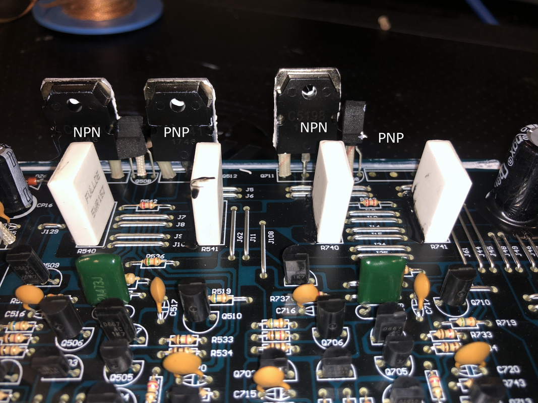
They are either ceramic spacers, ferrite beads or fibre glass impregnated spacers. If ferrite beads they help to reduce parasitic noise by introducing an inductance. If ceramic/fibre glass, they hold the transistor off the board at the required height for production and increase the mechanical stress required to damage the lead/component and board.
Last edited:
Definitely for production - set the device height during assembly (in lieu of a proper jig). This is low voltage so not for insulation. They are clearly not ferrite of course.
Having come across them plenty of times they are as Jon says----fibre glass impregnated spacers .
I used to see these all the time on old TV chassis on both transistors and diodes. It's like a woven heat resistance fabric tube.
Philips G8 and Thorn 3000 comes instantly to mind!I used to see these all the time on old TV chassis on both transistors and diodes. It's like a woven heat resistance fabric tube.
The issue is you can't mount the transistors to the heatsink first, as there are then too many leads to fiddle into the PCB. So you have to solder the transistors to the PCB and expect the mounting holes to line up with the heatsink's predrilled holes (we talking mass production here).
So by arranging the two outer legs of each power device to be a certain height the device will get soldered straight and level. The little devices are only glued to the heatsink so they only bothered with one sleeve for each of these to set the height.
All seems perfectly reasonable approach to mass production of an amp like this - surprized its not seen more often.
Philips G8 and Thorn 3000 comes instantly to mind!
Ah yes, we're going back a bit with those 🙂
Happy days.
After installing the new transistors it is obvious what these sleeves are for. It has nothing to do with performance, its just used as a "stop height" when inserting the transistors so they are sitting at the right height for mounting on the heatsink.
It is still no guarantee that there will be no stress on the leads after mounting. These sleeves are not precision parts.
The preferred method is to first mount the PCB to the heat sink, then insert the device into the PCB without soldering, mount the device to the heatsink and only *then* solder the device.
They may be sort of place holders but if they had any clue what they were doing, I bet that they were soldered as last.
Edit agree to Fusion916.
Jan
With straight pins there will be mechanical stress due to thermal expansion and contraction. That may make the solder joints go bad after a couple of years, unless those transistors rarely get hot during normal use.
Yes, good point. I solve that by making sure that the PCB is not rigidly fixed near those devices, so that the PCB can move a tiny bit during heating and cooling of the device.
Still doesn't solve it completely, I know.
Jan
Still doesn't solve it completely, I know.
Jan
The PCB isn't a rigidly mounted block of material so it deflects, i.e. bows slightly with even small up/down pressures including the thermal expansion cycling of the transistor leads in operation. It's only necessary to get the height approximately correct because your'e only minimising the stress on the joints at the solder setting temperature and that's as close as you can get since the board is flexible and presumably, only rigidly mounted at some distance from the point of leads attachment.
Last edited:
Why are there still guys who reject uploading images within this board? Sorry, I can't see the pic at the moment just because of that, hence am not able to think about it.
In former days I used to put plastic sleeves on the base and emitter legs of TO-3 devices to ensure proper insulation from the heatsink, especially with PTP wiring.
Best regards!
In former days I used to put plastic sleeves on the base and emitter legs of TO-3 devices to ensure proper insulation from the heatsink, especially with PTP wiring.
Best regards!
- Home
- Amplifiers
- Solid State
- What is the purpose of these bjt lead sleeves?