In a typical Lin topology amp or a symetical (2 LTPs, 2VAS's) variation, what are the factors or topology features that contribute to DC offset. I'm not talking about a serious offset, just within the normal acceptable range of 40mV or less. For example I have completed two working amps that appear identical. One shows an offset of ~10mV anf the other ~20mV. Even though this is "OK", I'm a little obsessive and think it would be nice if the offsets were the same AND as low as possible. (It's useless to tell me there is no sonic significance - I know that and still obsess.)
Are there component values that can be adjusted? Is there something that should be matched more closely? For example, the BJTs in each differential pair are matched for beta and their RE resistors are much closer than even 1% -- but the "top" and "bottom"
pairs are not to each other pair, etc. Or is matching the PNP/NPN pairs of output devices where one could look?
The first thing that causes bad offsets in this kind of amplifier is the LTP input stage. Being a differential amplifier, it is a servo incorporated to maintain the nullification of the amplifier output. If this stage is not balanced, the rest of the amplifier will obviously not be balance either.
The important part of the LTP is the two active devices, the transistors. If these have different gain, which they always do to some extent, they will reflect this difference by balancing differently. One way to achieve better offset is to incorporate a current mirror. This is done with the addition of two more transistors in the LTP. Also, matching of the transistors is very useful before deciding to add the mirrror if you have the ability to do so. There are ways to pad the balance of the circuit using a pot as well. This isn't generally accepted by the stringent audiophile circle, however, it is an easy way out. The real problem with pots being their inherent problems with age, heat, and dirt.
I have found that by adding a current mirror and by matching the transistors, output offsets under 5mV are not difficult to obtain. Many of my amplifiers are down to 1 or 2 mV if I spend the time getting all the kinks of the transistors worked out.
As far as the other stages in the amplifier, in most cases, they don't really have a great deal of effect on the balancing of the output offset. One more consideration I should note, is the matching of the feedback and input network resistors. It seems that by keeping the feedback resistor (one from output to LTP, not groung) matched with the bias resistor on the input side can help with balance. This because the LTP must reference through both of these resistors, one being tied to ground, and the other to the output, they must both give the same potential bias to the LTP or it will balance to the difference in the resistors, resulting in offset. In some amplifiers, I have seen 1% resistors used in these areas in order to maintain equal gain between channels for parallel and bridge operation, and also to achieve good offeset nullification.
I'm sure the real engineers here can offer much more detail into this situation, however, this is a chunk of the important theory I use in designing my own amplifiers, and it gives good results.
In the specific case, current mirrors are not an option. There are other areas where better matching may be possible.
What about top vs bottom matcing in the case of a 2-LTP input stage? Although each pair was pretty closely matched, it was not possible to match one pair to the other at all well with the stock of small sig BJTs I had on hand. They are not terribly expensive, so buying another batch or two until I could get a 4-way match do-able.
I was dubious about using a pot in place of the two RE resistors since with a 2-LTP topology, it would seem that you would need two pots which would be more likely to just confuse things.
When supply positive and negative voltage are different, that difference will appear.
The difference will appear at the output too.
This happens here, as i used to make my own transformer, and sometimes they are so well made that i have, as result, 400 mV differences between positive and negative rails.
regards,
Carlos
The difference will appear at the output too.
This happens here, as i used to make my own transformer, and sometimes they are so well made that i have, as result, 400 mV differences between positive and negative rails.
regards,
Carlos
One way;
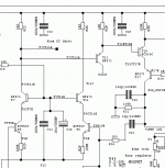
Here's one way Elektor did it with a double LTP.
Quite clever they adjust a small DC voltage right onto the input transistors of the DLTP. They use a trimpot and 2 x 10Mohm resistors. I have coloured* the relevant components in blue.
Cheers
* Australian / British spelling
Here's one way Elektor did it with a double LTP.
Quite clever they adjust a small DC voltage right onto the input transistors of the DLTP. They use a trimpot and 2 x 10Mohm resistors. I have coloured* the relevant components in blue.
Cheers
* Australian / British spelling
Attachments

I like the looks of the Elector scheme. Normally, I would be relectant to "monkey" with the input signal more than absolutlely necessary, but the high (M-ohm) values plus the cap (maybe parralled with larger cap -220uF-) ought to safely isolate the adjustment mechanism.
Since the two identicle amps share a common PS, the difference in offset between them can't be the whole story. Noetheless, I will check the rails more closely with a DMM having more digits. As it stands the look identical to 0.1V. If there is a difference, that provides an excuse to use one of ESP's circuits that force PS DC-offset almost perfectly to zero..
Since the two identicle amps share a common PS, the difference in offset between them can't be the whole story. Noetheless, I will check the rails more closely with a DMM having more digits. As it stands the look identical to 0.1V. If there is a difference, that provides an excuse to use one of ESP's circuits that force PS DC-offset almost perfectly to zero..
This use of a high value pot to null the amplifier is one that I've seen in Harman/Kardon equipment. Namely, the citation sixteen.
Being such a high value resistance, I can't really see it having any relevant effect on the signal information. And the system works very well for cutting out that last few mV of offset😉
Being such a high value resistance, I can't really see it having any relevant effect on the signal information. And the system works very well for cutting out that last few mV of offset😉
Most amplifiers from the seventies used a DC balance adjustment pot before op amp servos came to be. Very safe to do and will not colour (Candian spelling) the sound if done correctly. Matching the diff pairs will really help with DC offset and thermal drift. I recommend this first and do it myself when repairing or building an amp.
-Chris
-Chris
Then there is the question of stability and drift due to temperature shifts. Even thou' you try to match components (and I do that too) you can never match them 100%. Therefore there will be a slight chance of voltages and currents drifting resulting in a DC output also drifting. And here the DC servo comes in to take care of that.
Hi sam9,
Depending on topology of your amplifier, you may also have to look at the second stage of your amplifier, probably the VAS stage. Suppose the VAS is loaded with a current source (CCS), which is very common, then the VAS transistor should carry the same current as the current source (if the load of the output stage can be neglected or is symmetrical as well). Now, it is important that the VAS stage is designed in such a way that its base current is available from the input LTP when the LTP is in balance. The delivery of VAS base current should not cause an unbalance of the LTP, otherwise the overall feedback will offset the LTP just to get the right VAS current to match the CCS. This can be tuned (adjusted, tweaked) by changing the collector resistor(s) of the LTP.
In your double LTP topology, the positive VAS may have a different open loop current than the negative VAS stage. Overall feedback will then offset the LTP stages to get the two VAS currents equal. The solution is the same is above: adjust the collector resistor(s) of the LTP(s).
Steven
Excuse me Steven, but offset is created _only_ in the first stage of various reasons... if feedback is applied.
1 Different current gain
2 Different temperature
3 Different Vbe
This assumes a normal differential input stage. On top of that you can get additional offsets due to different DC resistance on non-inverting (input circuitry) and inverting inputs (feedback network).
You can say in short say that "internal" offset is always created but parts which are unequal where they should identical.
Hi Per Anders,
I do not agree that *only* the input matters. Take your headphone amplifier QRV01 as an example (http://home.swipnet.se/~w-50719/hifi/qrv01/index.html). I copied a part of the input circuit below.
Now, suppose you would reduce R22 (1k2) significantly, then in order to get the same VAS current through T15 (and through its cascode T17) it is necessary to offset the input LTP to get the same voltage across R22 again. Normally you would calculate R22 in such a way that if 50% of the LTP tail current is through R22, then the right VAS current is achieved. A smaller R22 (or bigger R30) requires, say, 66% of the LTP tail current to pass through R22 and T5 (and T7). Then the current through T9 (and T11) is only 33% of the LTP tail current, so the current division between T5 and T9 is 2:1, resulting in an offset of approx 20mV (at room temperature).
In case of a double LTP (symmetrical amplifier topology) this is less serious, since both halves may have the same (design) error. Then only the resulting VAS current will be different compared to its intended value, and no offset wil be created. But if there are differences between the top and bottom halve, also now an offset wil be created.
In case of the double LTP topology, it is also very important to match or adjust the tail currents of the LTPs.
Steven
Attachments
Steven, I think you have the wrong angle here.
Let's say that you have calculated everything and then look at things which really has influence on the offset. I assume that you don't mess with resistor values, just look at the transistors and then you have these three parameter I have listed.
A simple answer to sam9 is that extremly low offset is impossible to achieve with descrete parts but may be improved with monolithic transistor pairs like the very cheap BC847BS or more expesive one like SSM2210, SSM2220, MAT02 or MAT03. The big advantage of these transistors is close temp matching. I tested this in the amp you mention and also in QSXM2. I got a much less temp sensitive amp which was visiable if I monitored the DC-servo output which had to work much less.
I just tried to make clear to sam9, after he had indicated that he had done the utmost to select and match his input transistors, that unequal loading of the second stage or small design errors or tolerances could have influence on the offset too.
In his case also a mismatch between the tail currents of his double LTP could cause offset. This is also a nice place to adjust the offset (better than making the emitter resistors of the LTP unequal): adjust one of the tail currents.
In an Tandberg amplifier I've seen a DC offset correction circuit based on heating up the symmmetrical VAS stages. The two VAS transistors (positive and negative) where thermally coupled to two heating elements that were driven by a balanced amplifier, detecting DC offset. The LTP's were not affected.
Steven
n case of the double LTP topology, it is also very important to match or adjust the tail currents of the LTPs.
As a matter of fact, I noticed that the tail currents were slightly different. Although 1% resistors are used and each pair of transistors are matched to each other, I didn't have enough components on hand to do complete positive vs. negative (NPN/PNP) matching.
By the way, even an LT-Spice simulation shows some offset so I presume that is an indication that even "ideal" NPN/PNP pairs are not perfectly complimentary. (FYI, they are 2n5551/2N5401)
- Status
- Not open for further replies.
- Home
- Amplifiers
- Solid State
- What contributes to DC-offset?