Just delete R1 and its connections entirely, since the chassis ground is not defined,
and also is not in the schematic anyway.
and also is not in the schematic anyway.
In what part of the schematic I should connect the chassis GND? Near the power stage? And directly to GND or any component in series in the line?
The usual way is to designate a different ground symbol as the chassis ground.
There are several types to choose from, take a look in the Kicad library.
This would be the same symbol and net as for the IEC connector safety ground,
since the IEC safety ground terminal is always directly grounded to the chassis.
Then on the schematic, connect the 10R resistor lower end to that, if you still want to use the resistor.
Or you can connect the audio ground net directly to the chassis ground symbol.
Whether to use an impedance between the audio ground and the chassis depends on your design.
Sometimes the RCA input socket ground is elevated from the audio ground with 10R also.
This could be in addition to another impedance between the audio ground and the chassis.
Where on the schematic does not matter, since all parts of the audio ground net are the same.
It is a logical net, not a physical net. But it does matter where it's connected in the physical circuit.
Last edited:
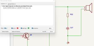
You have a +16 and -16 power pin, but you probably did not define it in the config dialog?
Not familiar with KiCAD, but in my Proteus there is a power setup screen where I would have to define: '16V power' or it will throw an error.
The idea is that you have defined all power points so that the layout module can catch errors.
The KiCAD help should explain. Can you find out which part is that #PWR09, probably in the netlist?
BTW R1 is shorted.
Jan

Jan is correct and in Kicad you need to attach a "PWR_FLAG" symbol to both the -48v and +48v power supply rails.
Its a special symbol for telling ERC where power comes from.
You can find this symbol via the menu "Place" then select "Power Port"
It may also be required to add a pwr_flag symbol to ground if the ERC keeps flagging power pin errors.
Its a special symbol for telling ERC where power comes from.
You can find this symbol via the menu "Place" then select "Power Port"
It may also be required to add a pwr_flag symbol to ground if the ERC keeps flagging power pin errors.
Last edited:
Many things wrong
Q3 no base connection
Q6/ Q7 both be NPN
which is shown in schematic but 4003 is pnp but shown as npn?
Dc current and operating point not even defined for Q5
needs baxandall diode for quasi operation.
Q6,Q7 need emitter resistors.
Load not connected, feedback not connected
wire shown, no connection
R9 not needed
R5 to high value.
R15, R19 value too high
no decoupling caps follow, not needed
I'm still in the learning process, I sure appreciate all the help you can provide, but some things are still hard for me to process.
Can you tell me if I'm on the right way to anything good? Or in the way of an explosive box?
I think I figured out some errors that you pointed out, but the Baxandall connection is still of a mystery to me.
here's what I got so far:

Can you tell me if I'm on the right way to anything good? Or in the way of an explosive box?
I think I figured out some errors that you pointed out, but the Baxandall connection is still of a mystery to me.
here's what I got so far:
Would a moderator be kind enough to move this thread to the appropriate section?
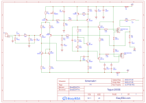
Here's what I got so far, I abandoned the previous design as it was not as good as I thought it could be and now I wish to know if there's any margin for improvements:
(Thanks in advance)

Here's what I got so far, I abandoned the previous design as it was not as good as I thought it could be and now I wish to know if there's any margin for improvements:
(Thanks in advance)
"There is no connection from the input stage to the driver stage."
Thanks... Duhh... I Could have I forget about that? LOL

Thanks... Duhh... I Could have I forget about that? LOL
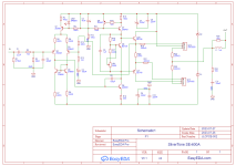
The negative rail is not connected to the power transistors. VR1 should not be able to short out the VBE multiplier because that would cause bias runaway. VR1 is put in the lower side of the VBE multiplier so that the failure mode is crossover distortion and not over current failure. But it must be wired so that the minimum resistance (R17+VR1) is about a 4x ratio (R17=1k/3=~330) , ie 4 diode drops for a 2EF output.
Input grounds 1 and 2 connect together and then through the ~10 Ohms to power grounds 3,4,5 and the missing ground on C7, C8, and the power supply. The input jack is floating, connected to 1,2 only.
R7, R8 may be too large for a single VAS transistor.
R7, R8 may be too large for a single VAS transistor.
- Home
- Design & Build
- Software Tools
- What am I doing wrong?