Dear Experts,
I need your corrections and optimization suggestions for attached square wave oscillator circuit.
This circuit is working on breadboard but if there is any scope for further optimiztion I'll incorporate it before proceeding to PCB layout.
Regards,
Sameer Dhiman
I need your corrections and optimization suggestions for attached square wave oscillator circuit.
This circuit is working on breadboard but if there is any scope for further optimiztion I'll incorporate it before proceeding to PCB layout.
Regards,
Sameer Dhiman
Attachments
I do not want to be too discouraging, but there is more than scope for optimization: first thing would be to drop the 4069 for another, much more suitable CMOS circuit: the 4047. It is an actual oscillator, having a decent stability and an exact 50% duty cycle (and low current drain).This circuit is working on breadboard but if there is any scope for further optimiztion I'll incorporate it before proceeding to PCB layout.
Even if the 4069 is non-negotiable, the circuit can be very much improved: for example, do not parallel the gates you did (they will simply increase the current consumption, the heating of the chip and instabilities), but use them for compensating the non perfect threshold of the other gates (or leave them unused, it will also be better).
The topology of the oscillator can also be changed for the better.
The output buffer should preferably not be linear since the upstream circuit isn't: a push-pull operating in digital mode will work better, have a lower consumption and a better fan out.
Could be a follower to keep things extra-simple, or common emitter for really good performances (also applies to the 4047).
But if you just want to build your own brew of circuit, why not? That's OK by me, but in this case, do not ask for opinions....
Thank you Elvee.
I built above circuit from parts which were lying in my box. The intention to build is to test audio amp.
Please forgive my limited knowledge/skills in electronics. I have few questions
1. How can I compensate the threshold of other gates ? Need the example circuit to visualize.
2. Example circuit of better topology.
3. How the push-pull in digital mode (assuming use of mosfet) give the option to control output level because they will acting as switches ?
A better topology is that of a function generator: the parameters and behavior are much more deterministic.1. How can I compensate the threshold of other gates ? Need the example circuit to visualize.
2. Example circuit of better topology.
3. How the push-pull in digital mode (assuming use of mosfet) give the option to control output level because they will acting as switches ?
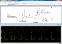
This is an example of such a generator, and it includes an automatic threshold compensation using one of the spare inverters, U3 and a few other components.
Here in the sim, the symetry isn't (yet) perfect, because the sim time was too short to allow for complete stabilization (C4 must be large enough to have a negligible effect at the lowest operating frequency).
Note that I have tweaked the 4069 model to exagerate its imperfection.
For most circuit samples, the polarity of C4 will be correct, but it might be reversed with a few others. The voltage will always be <1V, so it's not a big deal, but you can use a bipolar cap, or measure the actual polarity on the working circuit and correct it accordingly.
A bonus with this circuit is that you also have a triangle output, if you need it.
You are right about the OP buffer: with the level control, it cannot be digital.
It is posible to improve it significantly however
Attachments
This is the modified model:
And this is the unaltered one:
And here is the asc of the "skewed" generator:
Code:
.SUBCKT CD4069B  A Y  VDD VGND  vdd1={vdd}
 Rg  A 1 100
M2 Y 1 VGND VGND CD4069BN
M3 Y 1 Vdd Vdd CD4069BP
.MODEL CD4069BN NMOS (LEVEL=1 VTO=1 KP=0.9M GAMMA=3.97U
+ PHI=.75 LAMBDA=1.87M RD=20.2 RS=184.1 IS=31.2F PB=.8 MJ=.46
+ CBD=30P CBS=20P CGSO=40N CGDO=18N CGBO=50N)
.MODEL CD4069BP PMOS (LEVEL=1 VTO=-1 KP=2M GAMMA=3.97U
+ PHI=.75 LAMBDA=1.87M RD=28.2 RS=145.2 IS=31.2F PB=.8 MJ=.46
+ CBD=30.1P CBS=20P CGSO=40N CGDO=18N CGBO=50N)
.ENDS
And this is the unaltered one:
Code:
.SUBCKT CD4069B  A Y  VDD VGND  vdd1={vdd}
 Rg  A 1 100
M2 Y 1 VGND VGND CD4069BN
M3 Y 1 Vdd Vdd CD4069BP
.MODEL CD4069BN NMOS (LEVEL=1 VTO=1 KP=2.9M GAMMA=3.97U
+ PHI=.75 LAMBDA=1.87M RD=20.2 RS=184.1 IS=31.2F PB=.8 MJ=.46
+ CBD=30P CBS=20P CGSO=40N CGDO=18N CGBO=50N)
.MODEL CD4069BP PMOS (LEVEL=1 VTO=-1 KP=2M GAMMA=3.97U
+ PHI=.75 LAMBDA=1.87M RD=28.2 RS=145.2 IS=31.2F PB=.8 MJ=.46
+ CBD=30.1P CBS=20P CGSO=40N CGDO=18N CGBO=50N)
.ENDS
And here is the asc of the "skewed" generator:
Attachments
Elvee,
Would you mind heading over here to the Leader LFG-1300s
thread and see if you have any recommendations to make this
circuit a bit better with lower noicse and distortion?
http://www.diyaudio.com/forums/equipment-tools/269420-leader-lfg-1300s-doa-fix-then-upgrade.html
I'm thinking every little bit will help.
Currently I"m doing better than the .5 % (-46dB) spec that Leader publishes
at 0.18015% (-54dB).
I'm just not sure how much better I could make it with some simple
opamps or other IC/Fet tweaks.
- Status
- Not open for further replies.
- Home
- Design & Build
- Equipment & Tools
- Weekend Project: DIY Square Wave Oscillator based on CD4069