I've got only one DMM at hand.
Have anyone succeded biasing it with one instrument? Is it possbile?
Hi Siberia,
I only used one multimeter to adjust the Bias of VSSA, the first channel was a bit hits and misses.
The current thru the VAS increase with heat sink temperature, in my case it was 110mV (cold) to 165mV (hot heat sink).
I used the first channel as a reference,
1. Adjust TR1, measure the effective resistance of R9 to get 200R.
2. Adjust TR2, measure the effective resistance of R10 to get 200R.
3. Adjust TR3 so that the effective resistance about TR3 is about 530R.
4. Connect the VSSA to power supply, I also connect a light bulb in series to the primary of the transformer to limit the AC current - the light bulb should give a very dim red glow only.
5. Measure the voltage across TP1 and TP2, turn TR1 clockwise to increase the voltage - target is about 120mV.
6. Measure the output offset, connect the positive lead to output quik-on, Adjust TR2 until you get close to zero offset - turn TR2 clockwise to make the output more positive.
7. Disconnect the AC and light bulb.
8. If your meter can measure mA, connect the meter in series with the positive supply & the quik-on, turn TR3 clockwise to increase the MOSFET bias - the target is 182mA. Use LC's procedure as detailed in his supplement PDF in post #1547 if you cannot measure mA.
The VAS current will increase with heat sink temperature, so measure the voltage across TP1 & TP2 after the Heatsink is warmed up - I measure 165mV for HS temp ~ 55C.
Voltage across R7 = 15.5V (ccs current = 2.28mA)
Voltage across R8 = 16.0V (ccs current = 2.35mA)
LC may add with his comment for acceptable range for VAS and ccs current.
Happy building & enjoy the result.
Aaaah,  that might be very useful when I get home tonight. Huge thank you lot for the write up, sng001.
that might be very useful when I get home tonight. Huge thank you lot for the write up, sng001.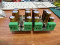
...it was 110mV (cold) to 165mV (hot heat sink).
if the heatsink gets really hot, I say you might have a problem..IMO
should only get very hot if you drive it really hard
Yes, those long hours to listen and compare, and feel a solution sound better with this record, and worse with this other one 🙂Guys, today's capacitors topic was the reason not to include capacitors in VSSA PCB set. Impressions which brand to use are so subjective that I simply left the decision to each individual.
Good luck 🙂When i get it working i will also try this :
Augmented Feedback Error Correction (AFEC)
Warning: get the fastest OPA you can find.
I am curious to see if your conclusion will correlate mines.
With listening time, you can try several changes and find some improvements. This don't mean the original schematic was wrong in any way. You can consider this as 'tuning'.Sorry, I cannot beleave this is true. Schematic has been changed and we are not informed.
Thanks, this AFEC project has zero priority but i found it interesting.
Bonsai himself sais that this technology can affect the stability of the amp and more testing is needed.
I know that ultra low distortion is not necessary to make a great sounding amp.
Bonsai himself sais that this technology can affect the stability of the amp and more testing is needed.
I know that ultra low distortion is not necessary to make a great sounding amp.
Schematic connections were not changed, only values of installed gate resistors are zero, again not by mistake. 😉
The very fact that circuit can be stable without gate resistors speaks a lot about quality of LC's circuit and pcb design. Jumper is far more linear than any resistor, including bulk metal foil. I think group buyers should be more than satisfied that instead of 100R and 68R gate resistors they have zero ohm jumpers on the board. This project is absolute success.
Hi ivanlukic and Esperado,
Is it to much to ask for a schematic that corresponds with the shipped product?
Note! I'm not questioning LC's design capabilities.
Btw, It's not just the absense of gate resistors, you now have small shunt caps from gates to ground.
Is it to much to ask for a schematic that corresponds with the shipped product?
Note! I'm not questioning LC's design capabilities.
Btw, It's not just the absense of gate resistors, you now have small shunt caps from gates to ground.
The current thru the VAS increase with heat sink temperature, in my case it was 110mV (cold) to 165mV (hot heat sink).
Hi, sng001...I would like to know how hot is hot ?...and size of heatsink ?
I'm not sure we agree on the situation. It is not a product. It is a project L.C did for himself.Is it to much to ask for a schematic that corresponds with the shipped product?
He was generous enough to share-it with us.
In a second time, he was kind enough to answer in a positive way to people asking, first for a printed board, second for parts and group buy, third for some components on boards. We (you) don't have to *ask*. Just thanks.
On a technical point of view, and my own opinion, the schematic he provided is PERFECT and working and the board was designed from it.
Now, L.C had made some little tunings on it after it was produced: would-you prefer he keep them secret, just for himself ?
Please, consider the original schematic as 'state of the art', and the little mods as 'tips'. You know ? The car out from manufacture, and the car you prepare for a race !
Now, L.C had made some little tunings on it after it was produced: would-you prefer he keep them secret, just for himself ?
Hi Esperado,
Short answer: No, since this is a GB.
I can only speak for myself and I have no interest in proceeding with this build right now until schematic is known. Either LC publish schematic or I or someone else publish the correct schematic. Believe or not, it will happen sooner or later.
In my village say '''clear sky lightning is not afraid'''
Giving the project is not big problem. Besides a technician having the board in his hands can analyze the circuit.
Giving the project is not big problem. Besides a technician having the board in his hands can analyze the circuit.
Hi, sng001...I would like to know how hot is hot ?...and size of heatsink ?
Hot means 55C, the heat sink that I used is a makeshift one - I used a old hard drive. I posted a picture in post #1456, I will mount the VSSA onto a proper heat sink. I just want to compare LC version with my homemade version.
@tinitus: I have collected some rough heat readings from my tests with Shaan's version of the circuit, and everything is pretty much as I expected from information here and in that other thread.
I expect the same with LC's "original" pcb, but I can measure again if anyone is interested. There are also pics with the heatsinks, etc., but I have already posted those too.
I expect the same with LC's "original" pcb, but I can measure again if anyone is interested. There are also pics with the heatsinks, etc., but I have already posted those too.
ok, thanks
55C is like exstreme classA
careful you dont loose it
might be close
55C should only be when driving 2ohm speaker
or else you are limited to 8ohm speakers
or could get into trouble already with just 4ohm
well, I tend to focus a lot on heatsink temperature
55C is like exstreme classA
careful you dont loose it
might be close
55C should only be when driving 2ohm speaker
or else you are limited to 8ohm speakers
or could get into trouble already with just 4ohm
well, I tend to focus a lot on heatsink temperature
Yes, I noticed those... or I should say a friend of mine did... (chuckle) I wonder if that is simply to balance the difference in native gate capacitance between N-channel and P-channel, when the gate resistors are reduced to zero?... Btw, It's not just the absense of gate resistors, you now have small shunt caps from gates to ground.
I also noted that a batch of the Alfets is held up because one of the pair of dies does not meet spec...
Btw, I have been told (not verified, but by a good source), that the gate capacitance is published in the "Typical" column with no min/max for a good reason, and to expect significant variation from one production run to another, from any manufacturer.
In any case, I don't think there are any secrets here, ... information overload is more like it. If I remember, LC explained about the fet p/n when I was confused by what was on the BOM. He could have just let that post lie, and let me look for the answer in among the 1500 posts in this thread on my own... 🙄
Not to mention that LC pops into Shaan's thread to encourage anyone and everyone who is making boards for free from his circuit, and to explain everything...
Hi ivanlukic and Esperado,
Is it to much to ask for a schematic that corresponds with the shipped product?
Note! I'm not questioning LC's design capabilities.
Btw, It's not just the absense of gate resistors, you now have small shunt caps from gates to ground.
OK. I agree. I think that LC should publish latest and final version of the schematic.
- Home
- Vendor's Bazaar
- VSSA Lateral MosFet Amplifier