Hi Andrej any audio gossip/talk/teaser from exhibition earlyer this month allowed here....Assembling three First One-s for the exhibition.....


 😉
😉

 .
.There were actually two exhibitons taking place in Ljubljana and in Zagreb.
I prepared three First One amps, all performed very well. Will post more later, with some interesting links. 🙂
I prepared three First One amps, all performed very well. Will post more later, with some interesting links. 🙂
Thanks for info......Will post more later, with some interesting links. 🙂
 ...
... for your new amp to succeed your expectation.
Pls confirm via email
Hi LC,
Please email me a confirmation and I can send you the payment and delivery details.
Thanks
Derek.
... but I'm receiving e-mails from other persons normally. No reports of undelivered messages up to now.
Give me your e-mail and your reply will work then maybe.
Hi LC,
Please email me a confirmation and I can send you the payment and delivery details.
Thanks
Derek.
Hi Mkusan,
I did the steps that you suggested but the best VSSA offset i got is 57mv with 300mv input bias. The question is : Can i use input bias at 300mv instead 120mv ? I have enought heatsinks for that.
I guess the sound is better now , the heatsinks are more hot too...
cheers,
I did the steps that you suggested but the best VSSA offset i got is 57mv with 300mv input bias. The question is : Can i use input bias at 300mv instead 120mv ? I have enought heatsinks for that.
I guess the sound is better now , the heatsinks are more hot too...
cheers,
I have not measured in real, for the moment, but it seems in simulations VSSA is very polished, and the bias values proposed by L.C. optimals for distortion.Can i use input bias at 300mv instead 120mv ? I have enought heatsinks for that.
10-15mA in the voltage amplifier stage are sufficient to drive the Mosfets Gates, even at ultra high frequencies.
If you enconter the same offset problems that Mkusan, i remember L.C. indicated to him the way to cure-it.
57mv of offset is 10 times too high.
Last edited:
Hi Mkusan,
I did the steps that you suggested but the best VSSA offset i got is 57mv with 300mv input bias. The question is : Can i use input bias at 300mv instead 120mv ? I have enought heatsinks for that.
I guess the sound is better now , the heatsinks are more hot too...
cheers,
I would keep input bias as suggested by Lazy Cat at 120mV.
Your offset is much better now but still a bit high.
Two things i would check in your place, are BC550-560 thermally bonded and compare results between TP1-TP2 and TP3-TP4.
Regards
Marko
Hi LC,
Please email me a confirmation and I can send you the payment and delivery details.
Thanks
Derek.
At the moment have just sent you an e-mail, hopefully succesfully. 🙂
I would look at the total idle current. Something does not seem right, and I would not try to fix it by leaving the bias so high. 30 mA current in the VAS transistors is about one watt dissipated in each TO-126.Hi Mkusan,
I did the steps that you suggested but the best VSSA offset i got is 57mv with 300mv input bias. The question is : Can i use input bias at 300mv instead 120mv ? I have enought heatsinks for that.
I guess the sound is better now , the heatsinks are more hot too...
cheers,
Out of my own curiosity, is this before or after the modification which was discussed three weeks ago? (this was the shorting of the DR in the supply rails)
LC, there are a lot of us who sadly haven't actually got VSSA kits that are trying to follow these very important and useful discussions .. especially about adjusting offsets & currents.
Without a schematic with numbered components & Test Points, it is impossible to work out what is going on.
Please, will you allow someone to post a schematic with component & Test Point numbers?
Without a schematic with numbered components & Test Points, it is impossible to work out what is going on.
Please, will you allow someone to post a schematic with component & Test Point numbers?
Just FYI, most of the useful documentation is linked in this post, by BYRTT:Without a schematic with numbered components & Test Points, it is impossible to work out what is going on...
http://www.diyaudio.com/forums/vendors-bazaar/225747-vssa-lateral-mosfet-amplifier-254.html#post3653117 Post 2534
The recent discussion about calibration refers to a couple sections of the Installation Document, link in first line of above post. This document also explains the test points. TP1 and TP2 are on either side of a 10R, so the 120 millivolts referred to above, corresponds to 12mA bias current flowing through a 10R, which is at the emitter of a 2SA1381 shown in V1.4 of the schematic, which can be found in post 300.
You basically have to print out the Installation Document, V1.4 of the schematic, and the BOM, and have them in front of you when you read the posts (at least that is what I have done). The couple parts missing from the schematic really have not come up here much.
Hi PMI, Thank you so much for show me sng001 procedure, these steps were the great tip,
1. Adjust TR1, measure the effective resistance of R9 to get 200R.
2. Adjust TR2, measure the effective resistance of R10 to get 200R.
3. Adjust TR3 so that the effective resistance about TR3 is about 530R.
4. Connect the VSSA to power supply, I also connect a light bulb in series to the primary of the transformer to limit the AC current - the light bulb should give a very dim red glow only.
5. Measure the voltage across TP1 and TP2, turn TR1 clockwise to increase the voltage - target is about 120mV.
6. Measure the output offset, connect the positive lead to output quik-on, Adjust TR2 until you get close to zero offset - turn TR2 clockwise to make the output more positive.
Now i got 120mv bias and 7mv offset in one channel and 120mv bias and 5mv offset in the other channel.
cheers
Hi,
I finally got some time to play with my VSSA, I had modded like on this post
http://www.diyaudio.com/forums/vendors-bazaar/225747-vssa-lateral-mosfet-amplifier-253.html#post3652831
All the setup went fine (those trimmers should maybe be of lower values since just barely turning them would make huge jump) and I just now saw that there is an error in the doc, measure accross 22R/5W resistor should be 4V and not 3.52V so this is easy to fix.
Now, what is the deal with the R23 resistor. I just saw a post that says to bypass it? Why and will this have an impact on adjustments, do I have to readjust bias, etc..? What if I keep the resistor in place?
http://www.diyaudio.com/forums/vendors-bazaar/225747-vssa-lateral-mosfet-amplifier-189.html#post3562049
One last thing, the amp is not yet in a chassis since it is on test. I'm getting a huge hum (ground loop) from connected to my equipment (tried 3 preamps, one DAC) but when connected to my iPhone it all works properly, total silence... Do I have to implement the star ground on schematics for testing?
Thanks
Do
Last edited:
See post #2534 for helpers (here link: http://www.diyaudio.com/forums/vend...lateral-mosfet-amplifier-254.html#post3653117). Regarding hum in hurry i see 3 tools, first in point 6 in that link you have access to Andrej's recommended grounding scheme, second R23 lift input ground by 10 ohm try shorting it on top or bottom PCB, and third the two screws for VAS devices carry ground loop up to PCB mayby try isolate it. Wish you good and fast troubleshooting.....Hi,
I finally got some time to play with my VSSA, I had modded like on this post
http://www.diyaudio.com/forums/vend...lateral-mosfet-amplifier-253.html#post3652831
All the setup went fine (those trimmers should maybe be of lower values since just barely turning them would make huge jump) and I just now saw that there is an error in the doc, measure accross 22R/5W resistor should be 4V and not 3.52V so this is easy to fix.
Now, what is the deal with the R23 resistor. I just saw a post that says to bypass it? Why and will this have an impact on adjustments, do I have to readjust bias, etc..? What if I keep the resistor in place?
http://www.diyaudio.com/forums/vend...lateral-mosfet-amplifier-189.html#post3562049
One last thing, the amp is not yet in a chassis since it is on test. I'm getting a huge hum (ground loop) from connected to my equipment (tried 3 preamps, one DAC) but when connected to my iPhone it all works properly, total silence... Do I have to implement the star ground on schematics for testing?
Thanks
Do
 ..........
Last edited:
Diode/resistor LC VSSA Mod
Today i visit a friend of mine (a another Diy fanatic). I decided to give a try to resistor/diode bypass mod. Clearly I mad a lot good to VSSA module in the bottom range. Yet VSSA play in the major league to my tast...i think i have to found good 42-44vdc power supply obtain a little more power from taht module.
Marc
Hi Do,
I had exactly the same with 10R ground-lifting resistor still in circuit: apparently total dead with no input cable, or with the input cable connected to battery powered equipment (FLAC player or battery powered headphone amplifier even while the later was connected to a DAC linked to the PC !!!), and varying levels of hum when connected to other transformer supplied equipment 😕. Why after removing it the hum disappeared? I have no logical explanation, unfortunately. For some reason, it allows unwanted signals to ingress in the amplifier via the GND connection 😡. I am very curious to find a logical clarification, and also why in other setups it has an improving effect.
So the steps you might want to follow should be:
1)Short out the 10R resistor on each channel's PCB
2)Remove the connection between the heatsink and the GND by mounting isolating washers over the holes for fixing the VAS transistors (I use 3mm screws so I could perfectly use here some TO-220 isolating plastic washers).
3) Connect each GND (Left channel GND and right channel GND) to the case in only one point, the same point you connect the Earthing/Safety Ground of the power connector/cable and on each channel in the point where GND spade connects to the PCB. I used here a DDRC circuit instead of a wire to preserve the separation between GND and power outlet and also between the two channel grounds. You can connect this chassis wire also in the point between the main reservoir caps, if you will find (as myself) difficult to insert 3 wires into one FASTON spade (the chassis wire, the supply GND and the Speaker GND) but ideally you should keep the shortest and thickest possible wire for the supply GND.
4) Mount the input connectors isolated from the case (chassis) and you are good to go. Of course, take care that the GND has no other connection to the chassis except at the GND FASTON.
Well, this was my recipe at least, I am curious if you find this solution working for you. Except the DDRC this is an implementation that matches Andrej's schematic for grounding, and he reported also a hum-free setup. Thanks to Andrej for this schematic and thanks BYRTT for making an index for some important posts in his #2534 ( I have a Chrome tab permanently opened to this page)
One more important observation:
In the test phase I assume you have the PCB mounted on the heatsink. Please use the chassis wire of the PCB (that you will later connect to the chassis) tied in some point to the heatsink during tests, otherwise you might trigger HF oscillation that will smoke/burn some 10R resistors in the Zobel filter. That can happen as heatsink will be capacitively coupled to the output ALFET and you can close the loop if you touch the heatsink and some sensitive circuitry of the input area in the same time. You don't have this problem before isolating the mounting screws of the VAS transistors (step 2), for obvious reasons. But please be aware of this.
Good luck and please report your findings, as I would like to hopefully confirm my experience! And sorry for this long post 😀
Last edited:
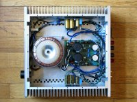
I have left the modules intact. Not made any of the mods so far, because I want to listen to them for a while first. Isolated from the heatsinks, from the start. Conventional ground, through the power supply board, and to a 10R to the chassis (earth).
They can be a bit sensitive to radiated noise when out of the chassis, and sitting in close proximity to the transformer, or the wires from the transformer secondary. Not very compatible with the Rat's Nest school of wiring, ... 😀
They can be a bit sensitive to radiated noise when out of the chassis, and sitting in close proximity to the transformer, or the wires from the transformer secondary. Not very compatible with the Rat's Nest school of wiring, ... 😀
Attachments
Thanks Pete! I see you are using a common supply for both channels, where this ground lift makes sense (in a way to avoid another ground loop within the source); have you tried hooking it to various sources to see if it works consistently hum-free?
- Home
- Vendor's Bazaar
- VSSA Lateral MosFet Amplifier