Hi everyone,
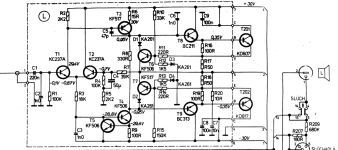
I'm troubleshooting this old TESLA amplifier from the mid 80's.
The person who sent me the amplifier stated that the midrange speaker sound distorted. On the video it almost sounds like the diaphragm is broken.
On the oscilloscope I found that at the powr amp secion there is a crossover distortion as you can see in the image.
I measured all the transistors and diodes. They are all fine. Also all voltages are as they should be.
The disortion can aready be seen at the base of T3.
Any idea what could cause it?
Thank you
Attachments
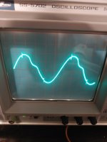
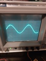
Yes, the first one was with the volume level bit up. Frequency 1k and about 1V - pp at the input of the preamp. no load connected in this case but the waveform looks the same with 8R load as well.
I’ll suggest a troubleshooting technique.
Sync your scope on the base of T3 as you’ve shown. Be sure to use x10 scope probes. Use second channel of scope to look for details in the output stages. The distortion defects in the output should be time aligned with glitches seen at the base. Poke around with second channel, using the good amp for reference when you see oddities. Scrutinize base-emitter behavior at output and drivers. With luck, you’ll gain insights to the problem.
Note that the T3 stage is approximately an integrator, so you’ll see 90 degree phase shifts between the two scope channels.
My best guess is deteriorated beta in an output transistor, but that’s a wild guess.
Good luck!
Last edited:

Do measure the voltages across R17 & R18. 0.95V (collector of T3) is not enough to forward bias two silicon junctions. Nor is 0.35V enough to bias one silicon junction. Same goes for the negative side. That amplifier is operating at best in class B, or even in class C.
If all the resistors and transistors seem to be ok, then increase the value of R8 until you see 10 - 15 mV across R17 or R18. Or better yet, add two silicon diodes (1N4148) in series with R8 (such that the diodes are forward biased) and reduce the value of R8 to get 10-15 mV across R17 or R18. The latter will add a bit of temperature compensation to the bias.
If all the resistors and transistors seem to be ok, then increase the value of R8 until you see 10 - 15 mV across R17 or R18. Or better yet, add two silicon diodes (1N4148) in series with R8 (such that the diodes are forward biased) and reduce the value of R8 to get 10-15 mV across R17 or R18. The latter will add a bit of temperature compensation to the bias.
That’s not crossover distortion. It is not at the zero crossovers. What happens at the base of a transistor should not be expected to be linear. It’s the output that matters.
TR3 base should not look like a pure sine (but it shouldn't have those kinks and distortion). The collector should look more sine like.The disortion can aready be seen at the base of T3.
Have you looked at the PSU with the scope? Make sure the rails are clean.
I had a big old JBL-Urei 6290 that exhibited very similar behaviour in your last pic. This only came apparent just before clipping. I guessed it was the protection transistors. I didn't investigate any further as I had other amps to work on at the time.
Remember it is a closed loop. Any issue will be seen everywhere.That’s not crossover distortion. It is not at the zero crossovers. What happens at the base of a transistor should not be expected to be linear. It’s the output that matters.
"I measured all the transistors and diodes. They are all fine."
Unless you tested all devices on a curve tracer at operating voltage you cannot be sure. I've found "leaky" output devices using a curve tracer that "normal" device testing wouldn't show.
I first screen in-circuit with a Huntron at the lowest voltage setting and then pull devices that that look suspect or surrounding components "mask" and use a real curve tracer.
At a minimum make an "Octopus" component tester.
I have no quarrel with the above comments.
However, note that current source T4 is controlled by base-emitter of T5, and that R8/R9 = 3.3. So voltage across R8 will be roughly 3.3 Vbe, thus providing some temperature compensation. I doubt T5 is thermally coupled to the heat sink, so temperature tracking is questionable. Perhaps thermal coupling of T5 could be improvised. Then trimming R8 would serve as a quasi temp-compensated bias adjustment.
BTW, I had it in my head that one of the channels was OK and was likely mistaken.
I just had the case of a 12k metal film 0.6W resistor which had decided to become non-conducting in a 30yo amp. The corresponding one in the other channel was already 14k instead of 12k. They were only running at 14mW in their position. Both looked completely normal, no heat signs.
So, almost nothing can be ruled out in terms of (partial) failure.
So, almost nothing can be ruled out in terms of (partial) failure.
- Home
- Amplifiers
- Solid State
- Vintage solid state amplifier troubleshooting