Great circuit! I have just tested it and it's really good! Very very loud, so i have to lower that otherwise gonna burn my headphones ")
I took 10ohm resistor in the R4 position and have like 90mA thru 2xBD139
I have +/-24V power in my setup and i wonder if this could be modified for 48V?
Does it make sense to do that?
I took 10ohm resistor in the R4 position and have like 90mA thru 2xBD139
I have +/-24V power in my setup and i wonder if this could be modified for 48V?
Does it make sense to do that?
Yeah, but over any simulation, is good to know what one is doing, because if not, you can't understand what the simulation is saying to you.
This is like an example, a professor told us in the university. Suppose you have a tester (VOM) that is malfuctioning. Suppose also that with this VOM you read 50V, for example, in the 220V power line. Do you touch the wires under those conditions?
This is like an example, a professor told us in the university. Suppose you have a tester (VOM) that is malfuctioning. Suppose also that with this VOM you read 50V, for example, in the 220V power line. Do you touch the wires under those conditions?

Have you tried it with the jfet current source to compare with the original design?
Yes, but not thoroughly tested. First impression was there was greater clarity at the high end.
The open loop gain was much higher as expected.
Note these comments pertain to using TIP41s as the output transistors, with the 2sc3852a's it sounded bad! Very muddy and distorted.
I used a J112 and a 180 ohm as the current source the current was around 10.5mA. I will probably try again with other jfets.
What warranty that both hemicycles receive equal amplifying factor (or gain)? The input transistor has a gain of about 10 (1200Ω collector/120Ω emitter). The upper final transistor is a follower, so gain ≈1. The lower final transistor ???
The 2SC3852 is extremely high current gain (guaranteed > 500), so there's a lot of feedback available. The circuit is dominated by feedback, and that transistor enables it to perform very well. The gain is stabilized by the feedback (masking imperfections of the output stage).
Give it a more linear output stage it will perform even better I suspect. The lower transistor is the obvious low-hanging fruit.
I got thinking about my last post and the possibilities of altering the output stage for this design. And then I got tinkering (simulator only though).
My thought was a CFP stage is pretty linear, so use a single-ended CFP with a passive load. Eventually I finished tweaking and came up with this:

Which seems to perform quite well. Of course the passive load resistor has to be chosen to handle the max current needed as it sets the output bias, and a 2907 isn't really upto the power dissipation needed.
The bootstrapped collector load for the first section cancels the Early effect and linearizes it. I set the input stage current much lower as it only has to drive a CFP stage at microamp levels.
The big disadvantage of these designs is the large offset voltage thump at switch-on, I would in practice go for a beefy opamp design, but as an exercise in design its a nice constraint to play with, 3 BJTs.
My thought was a CFP stage is pretty linear, so use a single-ended CFP with a passive load. Eventually I finished tweaking and came up with this:
Which seems to perform quite well. Of course the passive load resistor has to be chosen to handle the max current needed as it sets the output bias, and a 2907 isn't really upto the power dissipation needed.
The bootstrapped collector load for the first section cancels the Early effect and linearizes it. I set the input stage current much lower as it only has to drive a CFP stage at microamp levels.
The big disadvantage of these designs is the large offset voltage thump at switch-on, I would in practice go for a beefy opamp design, but as an exercise in design its a nice constraint to play with, 3 BJTs.
Attachments
The Noir headphone amplifier PCB sold in the diyAudio Store, also has a resistor for the "collector load" of the output transistor, called "passive load" above. In Noir's case the resistor is 68 ohms 12 watts, synthesized by a series-parallel combination of four pieces of (68R 3W) metal film resistors. They are mounted 7mm above the PCB and two holes are drilled in the PCB below each resistor, for improved airflow.
I did a bit more experimentation, realized I was loading the first stage too much, and reduced the series feedback so the shunt feedback was doing more of the work, and got THD < 0.01%:

[ R11 and R12 are increased substantially, ratio of R2 to R6 altered ]
Admittedly its a fairly small input signal, but it is into 30 ohms. I think I've reached the pinnacle of my three-BJT skills now.
The number of passives is partly making up for the restriction to only 3 transistors I think - more components in the signal path, better performance possible. Some people need to realise this
[ R11 and R12 are increased substantially, ratio of R2 to R6 altered ]
Code:
Fourier components of V(output)
DC component:0.00385879

Harmonic        Frequency        Fourier        Normalized       Phase          Normalized
 Number           [Hz]          Component        Component      [degree]        Phase [deg]
    1            1.000e+3        1.580e+0        1.000e+0        -179.86°           0.00°
    2            2.000e+3        2.642e-5        1.672e-5          13.98°         193.84°
    3            3.000e+3        2.407e-5        1.523e-5        -174.83°           5.03°
    4            4.000e+3        1.021e-5        6.461e-6          69.67°         249.53°
    5            5.000e+3        3.584e-6        2.268e-6          -8.53°         171.33°
    6            6.000e+3        2.323e-6        1.470e-6          -3.59°         176.27°
    7            7.000e+3        2.664e-6        1.686e-6        -154.55°          25.31°
    8            8.000e+3        2.464e-6        1.559e-6          65.76°         245.62°
............
   78            7.800e+4        1.639e-6        1.037e-6         120.27°         300.12°
   79            7.900e+4        7.995e-7        5.060e-7          45.89°         225.75°
   80            8.000e+4        1.477e-6        9.345e-7         121.55°         301.41°
Total Harmonic Distortion: 0.009598%(0.009594%)The number of passives is partly making up for the restriction to only 3 transistors I think - more components in the signal path, better performance possible. Some people need to realise this
Attachments
Last edited:
....the passive load resistor has to be chosen to handle the max current needed....
If you know what the load is, the optimum (most power for least dissipation) is with DC feed resistor 1.4X the load value and carrying 0.7X (not half!) the supply voltage. (Your 0.6 is not so far off, but your 180r reduces output even more than it reduces consumption/dissipation.)
So for 30 Ohms and 24V, use 42r and put 17V across it, 0.4 Amps, 10 Watts total dissipation in R and Q (which indeed smokes a TO-92). This puts up to 0.88 Watts in 30 Ohms, which is perhaps more than we should need.
With 14V across 180r your peak current is 80mA. 96 milliWatts at most. This is pretty good, though some ears and phones want more; 150mA is my reference but I have seen happy folks with currents ALL over the map.
30r loads do not need 24V supply! However 300r loads may. So it would be reasonable to aim the DC feed higher than 42 Ohms.
Mark's higher DC feed is a bit more economical and still gives very ample power for most headphones.
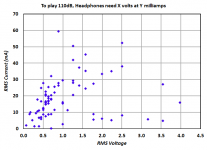
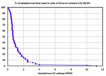
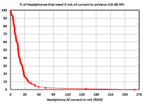
Good measured I-V data of 80+ headphones on this page:
Here are three ways to plot that data:
_
Here are three ways to plot that data:
_
Attachments
Mark + Mark, out of genuine curiosity to learn, Iam wondering why the choice of a passive load in the output stage is considered superior to a current source? I'm not disputing this choice just seeking clarification.
Whilst I'm at it, I have a question about LTspice. What is the figure in brackets with regards to THD?
Whilst I'm at it, I have a question about LTspice. What is the figure in brackets with regards to THD?
Last edited:
I don't recall anyone using the word "superior"
However I do recall seeing "3BJT" in the title of this thread.
I didn't mean to imply your circuit was either better or worse, just looking for more insight into the new ideas. I know that more complicated circuits can perform better, but I'm working with what I'm able to understand at this point and these circuits are graspable to a simple man like me!
- Status
- This old topic is closed. If you want to reopen this topic, contact a moderator using the "Report Post" button.
- Home
- Amplifiers
- Headphone Systems
- Very Simple 3BJT Headphone Amplifier