AKSA said:Zin of the BJT would be close to re, that is around 2.5R, and Zout of the mosfet would be recip gm, 40R for the ZVP1320F which has gm of 25mS.
Alex, since we are opeating at such low resistances where noise is no issue, would it be possible to use a PNP bipolar in place of the fet and simply interpose a 33R resistor between the two emitters?
With the superior gm of the PNP we would have very little error signal generated between its base and emitter, less than the fet, and the 33R resistor would swamp the non-ohmic Zout (again, 2.5R at 10mA) yielding far superior linearity.
While there would be a 70% voltage division with the 33R/82R resistors, the advantages would be similar OLG but superior linearity - and likely with some intrinsic damping making it easier to compensate.
Hugh,
there is one disadvantage: if you use BJT than the input impedance of the second stage reduced, lowering the OLG due to a lower gain in the first stage and introducing additional unlinearity due to the base current. In this case you'll have to use a buffer FET and this is a complication. I've tried it thought at the time and from what I've remember it did not improve things 🙂 . You'll need to use at least a darlington instead of a FET there to keep a similar OLG and I've tried it but liked FET version more.
I've used a similar topology VAS in my designs from about 1980 but this particular version has proved to work very well in many respects, including a relatively easy compensation for a particular O/S and a good sound quality too.
Cheers
Alex
Hi, Xpro,
What's the difference if the Drain of M1 (ZVP1320F) is used directly as VAS, not using R7 and Q8?
What's the difference if the Drain of M1 (ZVP1320F) is used directly as VAS, not using R7 and Q8?
AKSA said:.......
Zin of the BJT would be close to re, that is around 2.5R, and Zout of the mosfet would be recip gm, 40R for the ZVP1320F which has gm of 25mS. ...
Hi
Alex, nice circuit BTW.🙂
I may be wrong, but if the VAS acts like a differential and you added a small base resistor to Q8, it should then be in series with 're', so as to match the impeadance of the fet, and help it better act like a differential instead of a source follower driving a common base. 😕 or maybe an emitter resistor, or both?
If the VAS does act like a differential and the devices aren't matched, could there be a common mode difference voltage created across R7, and with the base fixed at VR18, create a distortion component?

lumanauw said:Hi, Xpro,
What's the difference if the Drain of M1 (ZVP1320F) is used directly as VAS, not using R7 and Q8?
It would 1) make it an inverter with a Miller type compensation and slow things down, 2) would at least require a cascode for the FET as it's output impedance is not very high and capacitances are fairly unlinear with voltage. And that would reduce available output swing etc. In my circuit voltages on the FET change very little which helps linearity. And 3) it would make the output current and voltage limits different for positive and negative polarities.
CBS240 said:I may be wrong, but if the VAS acts like a differential and you added a small base resistor to Q8, it should then be in series with 're', so as to match the impeadance of the fet, and help it better act like a differential instead of a source follower driving a common base. 😕 or maybe an emitter resistor, or both?
If the VAS does act like a differential and the devices aren't matched, could there be a common mode difference voltage created across R7, and with the base fixed at VR18, create a distortion component?
Just don't look at it as a differential 🙂 . It is not - it is more like a cascode. There are many ways you can change this 🙂 and as I've said earlier I did try different options. The very first one, many years ago, was a darlington instead of a FET, making it into a proper differential but I like the FET version more. As usual it may be because of a different character of residual unlinearities.
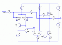
Here is a sketch of a topology I've used 25 years ago:
Cheers
Alex
Attachments
How well would this work with the current source load for Q2 removed and replaced with a simple resistor?
You would loose what, about 20dB open loop gain?
You would loose what, about 20dB open loop gain?
Hi DJK,
Yes, probably more than 20dB, with commensurate increase in distortion.
As I understand it, Alex's use of a FET coming off the current mirror is a strategy to maximise OLG of the input stage; replacement of the CM Q2 with a simple resistor would drop OLG of this stage to somewhere around Rl/re and drastically alter the gain relationships of his original concept.
The current mirror is no bad thing. They can sound very good if properly configured.
Cheers,
Hugh
AKSA said:a strategy to maximise OLG of the input stage; replacement of the CM Q2 with a simple resistor would drop OLG of this stage to somewhere around Rl/re and drastically alter the gain relationships of his original concept.
Hugh,
you are absolutely correct. It is a high gain of the input stage which provides very good linearity here. Replacing CCS load with a resistor would drop OLG by about 50 dB at LF and about 20 dB at 10 kHz according to the simulator.
Cheers
Alex
Gee, Alex,
I think I should start on another technology, I'm getting all the right answers now.....
Bit of a worry from someone with no formal electronics training....
No matter, I still can't configure a bloody PC to run Squeezebox, so I'm still pretty dim
Hugh
I think I should start on another technology, I'm getting all the right answers now.....
Bit of a worry from someone with no formal electronics training....
No matter, I still can't configure a bloody PC to run Squeezebox, so I'm still pretty dim
Hugh
AKSA said:Bit of a worry from someone with no formal electronics training....
No worries - I too have no formal electronics education 🙂 , just over 30 years experience and 3 year apprenticeship from a couple of great electronics engineers, when I was young. My degree is in physics and astronomy.
Cheers
Alex
Aha,
And here I show my prejudices, that would explain your focus on concepts and topologies rather than slavish measurements......
Creativity is definitely not a numerical process.....
Hugh
And here I show my prejudices, that would explain your focus on concepts and topologies rather than slavish measurements......
Creativity is definitely not a numerical process.....
Hugh
AKSA said:Aha,
And here I show my prejudices, that would explain your focus on concepts and topologies rather than slavish measurements......
Creativity is definitely not a numerical process.....
Hugh
Hugh,
in this case you are not quite right 🙂 .
my background in electronics for many years is in measurement equipment. I probably know more about all kinds of measurements than I do about audio. Because of that I do value measurements greatly, however I also know their drawbacks and problems, especially in the field of sound reproduction. I may add that different topologies are good for getting better measurements too, especially if you know what kind of result you are looking for, as "better measurements" are not the same thing as, say, "lower THD" 😉 . I use measurements extensively, as much as I could, however it is how you interpret them and how this corresponds to the final sonic performance (in case of audio), that what matters.
I would fully agree with what Nelson wrote here:
http://www.diyaudio.com/forums/showthread.php?postid=1238608#post1238608
"I like utra-low low distortion as well as anybody else, but it's not my boss."
Cheers
Alex
Alex,
Thank you for the kind rejoinder - it is very difficult to get to know someone's approach, let alone character, through the internet, althought the negative ones are quickly apparent.......
I agree with Nelson's comment emphatically. I think THD is appallingly simplistic, and much prefer to know individual measurements for H2, H3, H4 etc.
I do not agree with the bad rap global negative feedback receives. I think it's just fine and it solves more problems than it makes. The principle issue seems to be the extraction of the error signal; in most amps it is not accurate because of the highly non-linear transfer function of the venerable differential pair. By gunning for higher OLG in the front end we in fact minimise the error signal between the two input nodes, improving accuracy by remaining within the linear portion of the transfer function. I believe this is why your approach has such benefits; it's not just the higher feedback factor.
I quite like EC, but it's complicated, often requires setting up, and Self's much documented EF Type II seems to me to be the cat's whisker. Very little nasty distortion arises in AB output stages if the crossover transition is sharp.
I liked NP's comment about the mosfet suffering the foolishness of direct drive from the VAS. A very good point, I thought.
Thank you for sharing your novel VAS concept. I like it a lot.
Cheers,
Hugh
in this case you are not quite right.
Thank you for the kind rejoinder - it is very difficult to get to know someone's approach, let alone character, through the internet, althought the negative ones are quickly apparent.......
I agree with Nelson's comment emphatically. I think THD is appallingly simplistic, and much prefer to know individual measurements for H2, H3, H4 etc.
I do not agree with the bad rap global negative feedback receives. I think it's just fine and it solves more problems than it makes. The principle issue seems to be the extraction of the error signal; in most amps it is not accurate because of the highly non-linear transfer function of the venerable differential pair. By gunning for higher OLG in the front end we in fact minimise the error signal between the two input nodes, improving accuracy by remaining within the linear portion of the transfer function. I believe this is why your approach has such benefits; it's not just the higher feedback factor.
I quite like EC, but it's complicated, often requires setting up, and Self's much documented EF Type II seems to me to be the cat's whisker. Very little nasty distortion arises in AB output stages if the crossover transition is sharp.
I liked NP's comment about the mosfet suffering the foolishness of direct drive from the VAS. A very good point, I thought.
Thank you for sharing your novel VAS concept. I like it a lot.
Cheers,
Hugh
AKSA said:in most amps it is not accurate because of the highly non-linear transfer function of the venerable differential pair. By gunning for higher OLG in the front end we in fact minimise the error signal between the two input nodes, improving accuracy by remaining within the linear portion of the transfer function. I believe this is why your approach has such benefits; it's not just the higher feedback factor.
Hugh,
minimising the differential error voltage is equivalent to increase in OLG - just a different way to look at it. This circuit gives very high OLG and slew rate and at the same time fairly easy to compensate for stability.
AKSA said:Thank you for sharing your novel VAS concept. I like it a lot.
I'm glad you like it.
Cheers
Alex
Offtopic, but 🙂
You guys are both an inspiration. For a long time I wanted to go and study electronics at college (im 27)... but these days most colleges dont run such courses!
Most of my electronics experience is from "fiddling about". The maths has always scared the bejeesus out of me too.. it's good to know that you can become good without formal training 🙂
AKSA, conversely, I am great with PC's and software, and s*** with electronics in comparison 😉
Sorry for reviving an old thread. I've been toying with various cascode VAS configurations in spice when I found this beautiful idea here (high impedance load LTP -> CD -> CB VAS). After staring at the circuit with due appreciation I came up with the idea that LTP current source load can be replaced with a resistor between mosfet gate and source which forms a high impedance bootstrap-like load for LTP. Two transistors can be saved yet the OLG is still very large. One pitfall is that due to higher variation of mosfet threshold voltage that resistor may need to be adjustable for LTP current balancing. Is there anything else that I miss ?
Also I want to use a smaller clamp voltage for mosfet gate such that mosfet current in clipping mode is limited to slightly over 2x VAS current. Possibly using low leakage/capacitance ESD zener or reverse Vbe as a direct gate clamp to V+.
The amp I am simulating now is close to Alex's design with mods above, CFP output stage instead of darlington, shottky/cap filter for front end / VAS power (so I can get a bit more drive voltage riding the top of the PSU ripple at full power). I am also thinking of dropping separate voltages / filters for the mosfet and LTP tail current source (although I have to look at mosfet thermal mode).
I'll post the schematic in separate thread once I clean it up a bit (do not want to hijack this one). But my main question about LTP load can be visualized by looking at Alex's simplified diagram in the first post of the thread, removing LTP current source load and adding a resistor between mosfet gate and source.
- Status
- Not open for further replies.
- Home
- Amplifiers
- Solid State
- VAS with CD-CB stage