VAS, the design of a Virtual Accu System
Almost 10 years ago I noticed that, in my case and to my subjective perception, my phono preamp, my preamp and my D/A converter all sounded more harmonic when using batteries, while also producing a wider soundstage.
The experiments were performed with several lead acid batteries.
But since recharging these batteries every time after listening was rather annoying, I made some thoughts about what alternatives could be used instead.
One option would be to connect the batteries automatically to chargers when not playing, but this would ask for several intelligent chargers to prevent overloading plus some switching circuitry to connect and disconnect the chargers.
But finally the choice was made to simulate batteries with large caps, just like batteries not connected to mains, to be recharged in a subsonic frequency of 10Hz to avoid possible interactions with the audio signal.
The idea was to start with an commercially available external SMPS or Wall Wart supply that should load C1. After49msec this cap would have to be completely isolated from the external supply and left alone for 1 msec to recover.
Then as a next step this cap had to be connected with both sides to C2 to transfer a charge.
This floating Cap2 should be the one to fulfill the virtual battery function to be followed by a low noise voltage regulator giving a stable very low ohmic supply to the outside world.
After 49msec C1 should be disconnected again from C2, left alone for 1 msec to stabilise and then again reconnected to the supply from the external SMPS supply where the whole cycle starts again.

Now for the math. As an example, my D/A converter is specified to dissipate 12Volt at 10Watt or slightly less as 850mA.
What caps will then be needed for C1 and C2?
Starting with an external 18Volt SMPS supply, let’s assume that at the peak 16volt finally arrives at C2 because of internal losses in current limiting resistances. And let’s also assume that the power converter chips behind C2; needs a minimum of 14Volt input to generate it’s 12 Volt output.
That means that a 2 Volt voltage drop is allowed in 50msec.
With I=C*du/dt this would results in a 22mF cap.
I wanted to stay on the safe side and used 47mF caps, which should result in a 1 Volt sag when supplying the required 833 mA.
Measuring after having built the circuit, gave the following images on C2.

Fig 2, Voltage on C2 with the D/A converter connected to the TPS7A4700
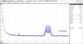
Magnifying the ripple resulted in Fig 3.

Fig 3, showing the AC ripple on C2.
Ripple on C2 is ca. 600mV, where from the down going slope it can be calculated that the current supplied to the DAC is C*du/dt or 47mF*0.6V/50msec = 560mA, much less as the expected 850mA.
After all C1 and C2 could have been three times smaller to still stay above the voltage regulator’s drop out voltage. But apart from a rather harmless additional dissipation in the voltage regulator, the bigger caps didn’t do any harm, so I left them in place.
So far for the theoretical background and checking it’s positive validity.
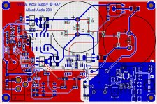
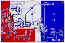
The final result is visible in both PDF’s attachments, one for the 12Volt Out with TPS7A400 and the second for a 18Volt Out without voltage regulator, but instead equipped with an extra Mosfet to isolate the external load in the start-up phase. The TPS7A4700 has an enable pin to do the isolation and therefore doesn’t need this additional Mosfet.
Input voltage for the 12Volt Out version has to be 18Volt In and for the 18Volt Out version 24Volt In.
Of course the 12 Volt version with TPS7A4700 can also be configured for 18 Volt or whatever voltage you need, and the one without voltage regulator has the same flexibility.
It’s just a matter of changing a few resistors, but the MCU is the same for all occasions.
Realisation, the problems to be solved
1) The selection of the switches. Relays have perfect isolation but are noisy, cause glitches when turned off and have limited amount of switch cycles, while when using Mosfets as switches, isolation from mains supply as large as possible is much more difficult because of Cds and Vds max but lifetime and silent (glitchfree) switching is guaranteed.
Mind you, with 10Hz the amount of switch actions is 315Mio times/year !
2) Second problem was to create a safe start up. When connecting a large cap to a supply, large inrush current will flow. Placing resistors in series will solve this problem, but once loaded these series resistors will have to be shortened.
3) Third item to solve was that the external load cannot be connected until enough voltage is available on C2, because during startup the series resistors will prevent C2 to get enough voltage with the load already there, so start up has to be done with no load connected.
Ad 1. I made a selection of SOT-223 Mosfets with less than 0.1R resistance, 4Amp continuous current although still having a Cds of several hundred picofarad when off. Quite likely after so many years their may be better alternatives for the used Mosfets with an even lower Cds, an important parameter to exclude noise from mains to feedthrough.
And because the floating SMPS supply has some capacitive coupling to mains resulting in a undefined state, it had to be prevented that large potentials could build up over the Mosfets because of that.
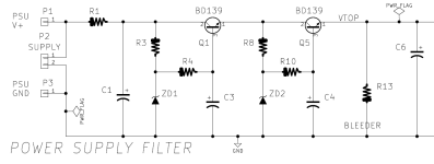
Looking at the 12 Volt PDF, that’s why around both caps C1 and C2 a network is added.
Around the first 47mF cap C1 this is R21, R22, R27, R25, R9 and C7. Around C2 the same network is added. Keeping all voltages now within controlled range, this keeps the noise rejection from the SMPS and from Mains well below 120dB, almost like isolated.
Ad2. A safe start-up was realised by sensing the voltage right before the voltage regulator, and feeding “Anode” and “Vout- back to optopcoupler U8.
Ca. 17 Volt between the two, will cause that T3-T4, acting as a thyristor will be switched on.
This in effect turns on Re1, causing the changing of the 22R serial load resistors into 0.3R.
The used IL221 is no longer available but it will not be too difficult to find a replacement.
Ad 3. The On-Off voltage on the thyristor is monitored by the MCU after division with R30-R40.
When this voltage on the divider is 3.45 Volt, the MCU will give a delayed release signal to the Voltage regulator and the current will start to flow.
To prevent any on off switching after release, the MCU has a hysteresis switching release off when On-Off gets below 10 Volt.
At the same time the MCU is responsible for generating the timing signals phase1 and phase2.
Important to mention but not visible in the circuit diagrams, is to connect the zero volt output from the VAS via a 10R resistor to Protective Earth.
To create a +/- voltage, just attach the positive output from one VAS to the negative output from the second VAS and connect this point via a 10R resistot to Protective Earth.
In the meantime several versions to feed my equipment are in use for at least 8 years without any flaws.
Hans
Almost 10 years ago I noticed that, in my case and to my subjective perception, my phono preamp, my preamp and my D/A converter all sounded more harmonic when using batteries, while also producing a wider soundstage.
The experiments were performed with several lead acid batteries.
But since recharging these batteries every time after listening was rather annoying, I made some thoughts about what alternatives could be used instead.
One option would be to connect the batteries automatically to chargers when not playing, but this would ask for several intelligent chargers to prevent overloading plus some switching circuitry to connect and disconnect the chargers.
But finally the choice was made to simulate batteries with large caps, just like batteries not connected to mains, to be recharged in a subsonic frequency of 10Hz to avoid possible interactions with the audio signal.
The idea was to start with an commercially available external SMPS or Wall Wart supply that should load C1. After49msec this cap would have to be completely isolated from the external supply and left alone for 1 msec to recover.
Then as a next step this cap had to be connected with both sides to C2 to transfer a charge.
This floating Cap2 should be the one to fulfill the virtual battery function to be followed by a low noise voltage regulator giving a stable very low ohmic supply to the outside world.
After 49msec C1 should be disconnected again from C2, left alone for 1 msec to stabilise and then again reconnected to the supply from the external SMPS supply where the whole cycle starts again.
Fig 1, the basic concept behind the VAS.
Now for the math. As an example, my D/A converter is specified to dissipate 12Volt at 10Watt or slightly less as 850mA.
What caps will then be needed for C1 and C2?
Starting with an external 18Volt SMPS supply, let’s assume that at the peak 16volt finally arrives at C2 because of internal losses in current limiting resistances. And let’s also assume that the power converter chips behind C2; needs a minimum of 14Volt input to generate it’s 12 Volt output.
That means that a 2 Volt voltage drop is allowed in 50msec.
With I=C*du/dt this would results in a 22mF cap.
I wanted to stay on the safe side and used 47mF caps, which should result in a 1 Volt sag when supplying the required 833 mA.
Measuring after having built the circuit, gave the following images on C2.
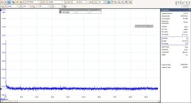
Fig 2, Voltage on C2 with the D/A converter connected to the TPS7A4700
As can be seen in Fig2, the average voltage on C2 is ca. 15Volt, more as needed for a TPS7A4700 LDO regulator, where in this case 13 Volt would have been enough.Magnifying the ripple resulted in Fig 3.
Fig 3, showing the AC ripple on C2.
Ripple on C2 is ca. 600mV, where from the down going slope it can be calculated that the current supplied to the DAC is C*du/dt or 47mF*0.6V/50msec = 560mA, much less as the expected 850mA.
After all C1 and C2 could have been three times smaller to still stay above the voltage regulator’s drop out voltage. But apart from a rather harmless additional dissipation in the voltage regulator, the bigger caps didn’t do any harm, so I left them in place.
So far for the theoretical background and checking it’s positive validity.
The final result is visible in both PDF’s attachments, one for the 12Volt Out with TPS7A400 and the second for a 18Volt Out without voltage regulator, but instead equipped with an extra Mosfet to isolate the external load in the start-up phase. The TPS7A4700 has an enable pin to do the isolation and therefore doesn’t need this additional Mosfet.
Input voltage for the 12Volt Out version has to be 18Volt In and for the 18Volt Out version 24Volt In.
Of course the 12 Volt version with TPS7A4700 can also be configured for 18 Volt or whatever voltage you need, and the one without voltage regulator has the same flexibility.
It’s just a matter of changing a few resistors, but the MCU is the same for all occasions.
Realisation, the problems to be solved
1) The selection of the switches. Relays have perfect isolation but are noisy, cause glitches when turned off and have limited amount of switch cycles, while when using Mosfets as switches, isolation from mains supply as large as possible is much more difficult because of Cds and Vds max but lifetime and silent (glitchfree) switching is guaranteed.
Mind you, with 10Hz the amount of switch actions is 315Mio times/year !
2) Second problem was to create a safe start up. When connecting a large cap to a supply, large inrush current will flow. Placing resistors in series will solve this problem, but once loaded these series resistors will have to be shortened.
3) Third item to solve was that the external load cannot be connected until enough voltage is available on C2, because during startup the series resistors will prevent C2 to get enough voltage with the load already there, so start up has to be done with no load connected.
Ad 1. I made a selection of SOT-223 Mosfets with less than 0.1R resistance, 4Amp continuous current although still having a Cds of several hundred picofarad when off. Quite likely after so many years their may be better alternatives for the used Mosfets with an even lower Cds, an important parameter to exclude noise from mains to feedthrough.
And because the floating SMPS supply has some capacitive coupling to mains resulting in a undefined state, it had to be prevented that large potentials could build up over the Mosfets because of that.
Looking at the 12 Volt PDF, that’s why around both caps C1 and C2 a network is added.
Around the first 47mF cap C1 this is R21, R22, R27, R25, R9 and C7. Around C2 the same network is added. Keeping all voltages now within controlled range, this keeps the noise rejection from the SMPS and from Mains well below 120dB, almost like isolated.
Ad2. A safe start-up was realised by sensing the voltage right before the voltage regulator, and feeding “Anode” and “Vout- back to optopcoupler U8.
Ca. 17 Volt between the two, will cause that T3-T4, acting as a thyristor will be switched on.
This in effect turns on Re1, causing the changing of the 22R serial load resistors into 0.3R.
The used IL221 is no longer available but it will not be too difficult to find a replacement.
Ad 3. The On-Off voltage on the thyristor is monitored by the MCU after division with R30-R40.
When this voltage on the divider is 3.45 Volt, the MCU will give a delayed release signal to the Voltage regulator and the current will start to flow.
To prevent any on off switching after release, the MCU has a hysteresis switching release off when On-Off gets below 10 Volt.
At the same time the MCU is responsible for generating the timing signals phase1 and phase2.
Important to mention but not visible in the circuit diagrams, is to connect the zero volt output from the VAS via a 10R resistor to Protective Earth.
To create a +/- voltage, just attach the positive output from one VAS to the negative output from the second VAS and connect this point via a 10R resistot to Protective Earth.
In the meantime several versions to feed my equipment are in use for at least 8 years without any flaws.
Hans
Attachments
Last edited:

Hans, I really like this well thought through and executed design. Thanks very much for sharing it.
I made a rough version of the same isolation technique based on a simpel flash light circuit (knipperlichtschakeling in Dutch) years ago. The resulting SQ was similar to your description given here.
One could also enhance further isolation by not using a smps, but an old fashioned linear supply, because the Cds capacitance of the switches in use, will couple RF more than LF. Just another way of getting more isolation, or at least not adding more.
Some lazy questions other DIY-ers are bound to ask sooner or later:
Are you planning on delivering boards or any service whatsoever?
Sincerely,
Marco
Hans
Thank you for communicating this with us. Very generous of you.
I am not one who can have a saying on this well thought-of design.
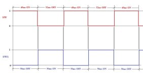
I would be satisfied with just a simple timing diagram of your idea.
Speaking of which I drew one just to know if I understood correctly your idea of the two switches never overlapping (this is based on the numbers in your description)
George
Thank you for communicating this with us. Very generous of you.
I am not one who can have a saying on this well thought-of design.
I would be satisfied with just a simple timing diagram of your idea.
Speaking of which I drew one just to know if I understood correctly your idea of the two switches never overlapping (this is based on the numbers in your description)
George
Attachments
Hi Marco,
Thx for your friendly feedback.
As for the feedthrough from the SMPS through the Cds, I have attached a few spectra taken from the SMPS entering the VAS, at resp. a 100Khz BW and a further magnified spectrum to show 50Hz and its harmonics.
Now look ate the same spectra from the 12Volt where leaving the VAS.
There is no sign of 50Hz and the horrible spectrum from the SMPS is also completely rejected.
Taking the -131.8dB noise level at the 14.9 Hz Bin width calculates into a 21uV noise level over 100Khz, a bit higher as the TPS7A47xx specified 4uV noise level, but this is because the scope's own noise is interfering and most likely the DAC is also backfiring some noise.
Regarding your second question: No, I'm not going into delivering boards, but when someone takes the challenge, he or she will get my full support.
Hans
Attachments

Hi George,Hans
Thank you for communicating this with us. Very generous of you.
I am not one who can have a saying on this well thought-of design.
I would be satisfied with just a simple timing diagram of your idea.
Speaking of which I drew one just to know if I understood correctly your idea of the two switches never overlapping (this is based on the numbers in your description)
George
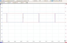
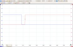
Here you see the combined phase1 and phase2 signals in the first image.
Because the gaps between the two are hard to see, I have magnified bot gaps.
Hans
Attachments

Hi Mr. Polak. Did you also try LCLC filtering (so not CLC) with linear power supplies? The results resemble using lead acid batteries.
Hi Jean-Paul
I tried lots of filtering systems, just to replace Bel Canto’s expensive virtual battery system, equiped with lots of L’s and C’s after each other, but to my subjective perception this VAS sounded by far the best of them all.
Hans
I tried lots of filtering systems, just to replace Bel Canto’s expensive virtual battery system, equiped with lots of L’s and C’s after each other, but to my subjective perception this VAS sounded by far the best of them all.
Hans
Us monolithic CMOS chaps would be likely to call that a "switched capacitor filter", which is a topic with large amounts of theoretical and practical research, and much published literature.
Among the second order effects which plague switched capacitor filters, is a problem called Clock Feedthrough, in which the Cgs and Cgd of the switching MOSFETs, couple the rising and falling edges of the (10 Hz in your case) clock signal, onto the output. An undesirable result. One simplistic approximation of a fixup is to use pairs of complementary MOSFETs for your switches (so called Transmission Gates), so that every switching event includes both a rising clock and a falling clock. Voila, if you can match (Cgs_NMOS == Cgs_PMOS) and (Cgd_NMOS == Cgd_NMOS) and (rising edge waveshape == perfect_inversion of falling edge waveshape) then, it naively appears, you can reduce or nearly eliminate Clock Feedthrough.
There are other second order effects and fixups thereto; this is just an introduction to the tip of the iceberg.
Last edited:
Thank you.Hi George,
Here you see the combined phase1 and phase2 signals in the first image.
Because the gaps between the two are hard to see, I have magnified bot gaps.
Hans
It seems I got it right. Your screenshots show a gap of 0.5ms which is fine as a result of practical implementation.
George
Would it be possible in theory and practice to use supercapacitors or ultracapacitors for this application?
@Hans, I didn`t expect that much attenuation, excellent!
Is this attenuation depending much on the connection of the VAS to protective earth?
@mark, I thought clock feedthrough was only a problem in e.g. dc to dc converters where the clocks used can be in the megahertz range? If it is an issue here, could soft coupling of the Gate (change Resistor R3 and R4 to several kilo ohm, use a ferrite bead) fix the issue?
btw, shouldn`t it show up in the measurement Hans did in post #5, or is the setup not suited (common mde signal)?
For super capacitors it might be interesting to know the minimum voltage the circuit still works, as most supercapacitors already need balancing circuits above 2,7 volt, as well as the fets needs to cool them
Us monolithic CMOS chaps would build a test vehicle / prototype and measure it. After, of course, running tons of circuit simulations to optimize the test prototype's (simulated) performance.
I have no idea what effect the PE connection to the zero volt output causes, but since everything is floating, I don’t think it contributes to the the large attenuation. But it’s main reason is to give the VAS casing a shielding function and to bring the zero volt output at the same level as in the D/A converter.@Hans, I didn`t expect that much attenuation, excellent!
Is this attenuation depending much on the connection of the VAS to protective earth?
@mark, I thought clock feedthrough was only a problem in e.g. dc to dc converters where the clocks used can be in the megahertz range? If it is an issue here, could soft coupling of the Gate (change Resistor R3 and R4 to several kilo ohm, use a ferrite bead) fix the issue?
btw, shouldn`t it show up in the measurement Hans did in post #5, or is the setup not suited (common mde signal)?
Hans
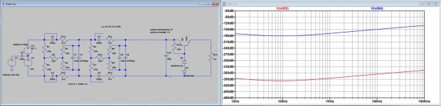
Hi Mark,Us monolithic CMOS chaps would build a test vehicle / prototype and measure it. After, of course, running tons of circuit simulations to optimize the test prototype's (simulated) performance.
That’s exactly what I did, simulate the circuit trying to find the sensitivities.
I found a suppression of at least 120dB up to 100Khz before the the voltage regulator on Q1's collector in blue.
Mind you, IMO this is not a switched capacitor filter, it's a DC transfer circuit.
Hans
Attachments
Last edited:
I use similar circuits myself, to smooth the DC applied to power amp front end circuits. I prefer a (R+ZD+R+C+Q) version as shown below. This schematic happens to put two of them in cascade for extra attenuation. BTW if your voltage headroom budget can deal with it, installing a shielded inductor in series with R1 is helpful too. Just be sure to choose an L such that SQRT(L/C1) < 1.5*R1 so the LC resonant circuit is well damped.
I wonder whether your "generic NPN" transistor has any Early effect (dIce/dVce > 0) in its SPICE model. Early effect is one of the limiting factors in these circuits.
_
I wonder whether your "generic NPN" transistor has any Early effect (dIce/dVce > 0) in its SPICE model. Early effect is one of the limiting factors in these circuits.
_
Attachments
Last edited:
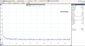
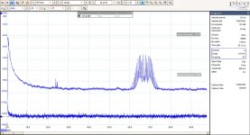
To make things probably even more clear, I have added the measured SPMS input voltage and the 12Volt output voltage in one image at exactly the same scale.
No early effect or whatever as a limiting factor, this it the real world.
The Scope's noise is at -136.7dB, so in fact the 12 volt has a noise at -133.5dB @ 14.9 bin-width or 55nV/rtHz.
Hans
No early effect or whatever as a limiting factor, this it the real world.
The Scope's noise is at -136.7dB, so in fact the 12 volt has a noise at -133.5dB @ 14.9 bin-width or 55nV/rtHz.
Hans
Attachments
I think that's a fantastic graph but the linear-scale horizontal axis is nonintuitive. Could you explain please?
Also is the variable of interest the delta-Y between the two curves? Output (bottom curve) minus input (top curve) since both are in dB units?
Also is the variable of interest the delta-Y between the two curves? Output (bottom curve) minus input (top curve) since both are in dB units?
- Home
- Amplifiers
- Power Supplies
- VAS, the design of a Virtual Accu System.