Hello everyone,
I have been reading a lot about audio power amplifiers and general op amp design. I feel like I have a pretty good grasp on the basic operation of the input stage as well as the output stage. I am having a bit of trouble understanding the Voltage-Amplifier Stage (VAS) though. I have been reading the Audio Power Amplifier Design Handbook by Douglas Self and there is a great explanation on page 120. The VAS is simply a current controlled current source which means you need some kind of load to translate the current into a voltage. This voltage is typically split across a VBE multiplier (to set the operating region of the transistors) then fed into a unity gain output stage.
This seems very simple and straightforward but I am having some difficulty translating this into an actual design. I have seen several designs that use bootstrapping resistors [High Quality 60 Watt Power Amplifier, 20 Watt Class-A Amplifier], and on Wikipedia’s page for the Operation Amplifier [Operational amplifier - Wikipedia, the free encyclopedia], the VAS uses a current mirror load with current set by a 39kOhm resistor.
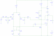
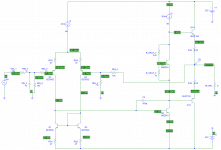
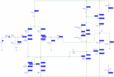
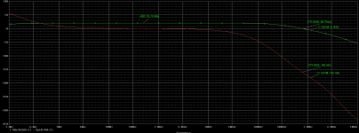
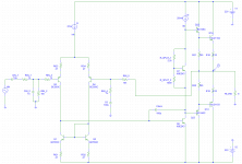
The issue I keep running into is related to biasing (I am pretty sure). The voltage at the collector of my VAS transistor seems to sit too high or too low and my simulations result in a high DC bias at the output. I am using a SPICE current source, which is probably a bad idea. However, with an ideal current source the load impedance of the VAS stage should be rce of the VAS transistor in parallel with the input impedance to the two output transistors. I have included my schematics with DC biasing (both voltage and current). I also included the gain output (as well as phase). The marked points are the max gain (in dB) as well as the gain and phase margin. If anyone has any ideas on what is going on with the DC bias at the output I would be interested to hear about it.
Thanks,
Waddy
simplify the system you are trying to understand and analyse.
Replace the mirror with a pair of resistors.
Set up the LTP so that the Ie values are identical in the two halves.
For this "understanding" to happen throw away the simulator and do it with pencil and paper and a calculator to calculate the currents.
Currents are very important.
I have said this many times before:
A simulator that is written by someone else that includes many unknown formulae hides the answers you need.
You need to understand what is happening to allow you to ask the sim the correct question to get the answer you need.
There is little chance you will come up with the right question when you don't understand how the circuit works.
Go back to basics.
Looking at your simple schematic (first picture) it looks rather good. Now those MJ21193/94 power transistors are hungry. They need quite much current especially when the output swing is heavy.
You should add two drivers from VAS to the two power transistors. These drivers will act as buffers and will only take little current from VAS.
Suitable drivers are TO-126 transistors like BD139 and BD140
You should add two drivers from VAS to the two power transistors. These drivers will act as buffers and will only take little current from VAS.
Suitable drivers are TO-126 transistors like BD139 and BD140
Adding a capacitor in series with RIN_4 should fix the DC offset. Something like 100uF would be good.
Hi Waddy,
Lineout and Godfrey have it.
Interpose drivers after the bias generator and the output stage. BTW, replace the 1K be resistor with a trimpot so you can set the quiescent. The 211s have low beta and need boosting, a VAS cannot drive them alone. BD140/139 are excellent suggestions.
Lastly, you have 500pF as your Cdom between c and b of the VAS. This will over compensate the amp and deliver a leaden, slow sound quality. Reduce it to 100pF, then try 82p and then 68p. You can predict the dimension but it's very complex with utility PSpice programs. Empirical is best.....
Cheers,
Hugh
Thanks for all the great replies! I had to work a last minute second shift yesterday to finish a project at work 🙁, so this has been the first time I have been able to check the feedback.
I started with the comments by godfrey. That capacitor dropped the DC bias from 202mV to 5mV. That is a huge improvement. Thinking about the effect this capacitor should have has led me to the following conclusion. Since the output impedance of the amplifier should be close to 0, we can assume that the feedback resistors RIN_4 and RIN5 are seen in parallel from the base of Q4. This leaves only 909 ohms on the base of Q4 where Q3 actually sees closer to 11k (at the DC condition). If I add the 100uF capacitor in series with RIN_4, the impedance seen from the base of Q4 is 10k, much closer to what the base of Q3 sees. I tried an 11k resistor for RIN_5 and the DC offset measures a bit lower, about 3.3mV. With a value like 100uF, that capacitor should have little to no effect at fairly low frequencies, meaning no effect on the midband gain.
I also added the BD139/140 to the output stage as a second unity gain buffer. At DC, the output stage draws only uA from the VAS instead of close to 10mA. That seemed to make the VAS a lot happier!
Cdom changes the slew rate, and the smaller the capacitance the better. I plan on adjusting Cdom for a phase margin between 45-55. I reduced Cdom to 100pF and everything looks fine so far. I plan on adjusting it when I have a bit more time to really see the effects. Also, the bandpass filtering at the input to the amplifier seems to help a little with instability.
Thanks again for all of the exceptional help! I really learned a lot this morning reading everyone's comments. I am including the current circuit with this reply.

- Status
- Not open for further replies.
- Home
- Amplifiers
- Solid State
- VAS Biasing
