More than willing to help!
Can you tell me what this circuit will be powering? I am geussing a pre-amp, but not certain. If it is a pre-amp, will you be using high-open loop op-amps, or a very simple class-A circuit. The reason I ask, is that op-amps may give you a good deal of inherent power supply rejection. A simple class-A preamp without a lot of feedback will require a much better level of regulation.
Can you tell me what this circuit will be powering? I am geussing a pre-amp, but not certain. If it is a pre-amp, will you be using high-open loop op-amps, or a very simple class-A circuit. The reason I ask, is that op-amps may give you a good deal of inherent power supply rejection. A simple class-A preamp without a lot of feedback will require a much better level of regulation.
G -
Asking here feel real weird. ...
I am still a little puzzled by the use of two transistors, are you doing something that Jorgensen did in his version 2 of his headphone amps? To provide accuracy and speed. (???) I really don't know how so either. Might be asking a dumb question. (In that case, you may kick me!
My version still uses LM317. I have been stripping parts off it. ...
Tomo
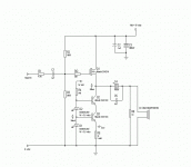
Actually Tomo I got the idea off of a schematic I saw. I beleive that this is what you would call a SS version of the bottlehead CCCS. I changed the PNP's to NPN's and used lower voltage BJT's but it is essentially the same circuit. I figured that if it will work on tube amps it will work on SS amps. The guy who thought of it knows more than I will probably ever know about electronics so I figure that it will get the job done.
Arrgh,
My curiosity not satisfied, must understand ... must understand ...
Hey you still got Mr Bottleheat's manual? It must say something.
Tomo
My curiosity not satisfied, must understand ... must understand ...
Hey you still got Mr Bottleheat's manual? It must say something.
Tomo
Never bought the manual Tomo. I used the diagram I found on the web. Maybe one of the more learned will jump in and explain. I can't. I understand how to bias it but not why two bjt's are better than one. Sorry.
brain damage
Tomo,
Your emiticon is giving me a
I'd better attempt an explanation in the interests of your health.
G mentioned this was borrowed from a valve circuit. Usually when trsnsistors are cascoded like this it is often either a) to have a higher performance but lower power/Vce BJT on the bottom, shielded by a lower performance, higher power/Vce BJT above or b) to reduce the Miller effect of Ccb of the lower BJT.
In this case it seems that option b) is unlikely because the Ccb of the upper BJT feeds straight back to the base of the lower BJT - so no benefit. If this was originally part of a valve design, with correspondingly high voltage swings, it seems plausible that option a) is the answer and that originally the the upper BJT was a different transistor to the lower one.
BAM
So using two BJT's has no benefit in this application? I guess that I can eliminate one of the BJT's and just use one transistor and one LED. Thanks.
Hello,
Tomo's eye opened as if he has received the enlightment. And there was full of rejoicing!
Thank you, BAM.
Tomo
Tomo's eye opened as if he has received the enlightment. And there was full of rejoicing!
Thank you, BAM.
Tomo
Tomo said:G -
Asking here feel real weird. ...
I am still a little puzzled by the use of two transistors, are you doing something that Jorgensen did in his version 2 of his headphone amps? To provide accuracy and speed. (???) I really don't know how so either. Might be asking a dumb question. (In that case, you may kick me!
My version still uses LM317. I have been stripping parts off it. ...
Tomo
The 2nd transistor is a cascode and will make the current source
more ideal, or, approach infinite impedance.
Terry 🙂
As Terry points out you can adjust this circuit to make the CCS more ideal. You need to disconnect the base of Q2 from the bias chain for Q1. Then have a separate bias for Q2 base referenced off, say, the -'ve rail. A couple more parts needed for this.
The principle here is as follows: an ideal CCS has infinite impedance as you know. So this means the Ic of Q3 must be constant regardless of variations in Vce. This in not achievable in practice because of the limitations of transistors. One of the main problems is the Ccb that must charge up and down as Vcb changes, and this creates a Miller effect that effectively multiplies the effect of Ccb and reduces the impedance of the CCS, moreso as frequency rises. You could stop this by holding Vbe perfectly constant (caps and regulation) - but this is not as easy to do in practice. And you still have a Cce effect that makes a small contribution. When you shield using Q2 the CCS impedance tends to reduce to the value of Cbc of Q2. But since Q2's emitter current is set by Q3 you don't get the Miller effect.
The principle here is as follows: an ideal CCS has infinite impedance as you know. So this means the Ic of Q3 must be constant regardless of variations in Vce. This in not achievable in practice because of the limitations of transistors. One of the main problems is the Ccb that must charge up and down as Vcb changes, and this creates a Miller effect that effectively multiplies the effect of Ccb and reduces the impedance of the CCS, moreso as frequency rises. You could stop this by holding Vbe perfectly constant (caps and regulation) - but this is not as easy to do in practice. And you still have a Cce effect that makes a small contribution. When you shield using Q2 the CCS impedance tends to reduce to the value of Cbc of Q2. But since Q2's emitter current is set by Q3 you don't get the Miller effect.
Hi Trader,
I kind of understand what you are saying. I can bias the base of Q2 from a different point. What is the -'ve point that you are refering to? Are you saying to bias Q2 and Q3 separately from VDD? Each having it's own current limiting resistor, it's own LED and current adjusting resistor? I'm sorry if this seems like a dumb question but I don't quite follow what you are saying. Unfortunately I'm not in your league as far as designing and understanding goes but I'm trying to work through it. I did intend to place a cap from base to ground on Q2 and Q3 in order to reduce noise and maintain peak voltage.
I kind of understand what you are saying. I can bias the base of Q2 from a different point. What is the -'ve point that you are refering to? Are you saying to bias Q2 and Q3 separately from VDD? Each having it's own current limiting resistor, it's own LED and current adjusting resistor? I'm sorry if this seems like a dumb question but I don't quite follow what you are saying. Unfortunately I'm not in your league as far as designing and understanding goes but I'm trying to work through it. I did intend to place a cap from base to ground on Q2 and Q3 in order to reduce noise and maintain peak voltage.
G,
Sorry, I tend to be brief to the point of incomprehensibility most of the time. I'm the same in spoken communications too.
By -'ve I meant 0V labelled on the schematic.
Yes, bias the base of Q2 separately. The other Q2 connections remain un changed (so you don't need a second current-limiting resistor). You could duplicate the LED chain for example as you suggest. Also, as you observe, slap a cap between Q3 base and 0v and one between Q2 base and 0V. Say 100nF ceramic. The cap will help reduce signal coupling through the Cbc of each transistor. If I've been clear you will notice that you only need one LED for biasing Q2 in this arrangement.
Thanks Trader. I'll redo the diagram and post it to see if I understand what you are saying. I believe that you mean that Q2 will have it's own LED and LED current limiting resistor to VDD with a .1uF ceramic cap from base of Q2 to 0v and the cathode of the LED to 0v. The same goes for Q3. All of the other connections will remain the same. Thanks.
traderbam said:As Terry points out you can adjust this circuit to make the CCS more ideal. You need to disconnect the base of Q2 from the bias chain for Q1. Then have a separate bias for Q2 base referenced off, say, the -'ve rail. A couple more parts needed for this.
The principle here is as follows: an ideal CCS has infinite impedance as you know. So this means the Ic of Q3 must be constant regardless of variations in Vce. This in not achievable in practice because of the limitations of transistors. One of the main problems is the Ccb that must charge up and down as Vcb changes, and this creates a Miller effect that effectively multiplies the effect of Ccb and reduces the impedance of the CCS, moreso as frequency rises. You could stop this by holding Vbe perfectly constant (caps and regulation) - but this is not as easy to do in practice. And you still have a Cce effect that makes a small contribution. When you shield using Q2 the CCS impedance tends to reduce to the value of Cbc of Q2. But since Q2's emitter current is set by Q3 you don't get the Miller effect.
I think you are confusing things here. The original circuit is fine
and the base ref points are fine as drawn using LEDs as
ref points. You can put some hi qual EL caps across LEDs to
reduce what small noise they contribute. To minimise miller effect
choose Q2 with small miller cap say less than 10pF and the
current source will work great and have very good BW.
Terry
Gavin, yes that is basically what I meant. I'd put another LED or a series diode in the Q3 bias to make the Vce of Q4 is a little higher.
Terry, yes this is probably over-complicated for the application of a headphone amp. I think you only really need one transistor and it'll sound fine. My premise was that if two transistors are desired by the perfectionist (to shield the lower transistor from the effects of output voltage swing) then you might as well do the job properly.
Terry, yes this is probably over-complicated for the application of a headphone amp. I think you only really need one transistor and it'll sound fine. My premise was that if two transistors are desired by the perfectionist (to shield the lower transistor from the effects of output voltage swing) then you might as well do the job properly.
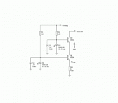
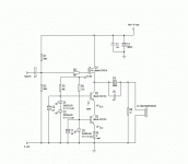
Hi Trader. This seems a little complicated but it wasn't too much trouble to incorparate it into the PCB so I went with it. Hope this is what you are talking about. It looks right to me. I don't quite follow the need to increase the Vce in Q3 by adding the extra LED in the Q2 bias. Would you mind explaining how this improves the CCS? The 1uF electrolytic bypass caps in the CCS are going to be Black Gate N series bipolars. They work very well for bypassing from what I understand.
Attachments
lily-gilding
One other thing you could consider, if you want to take this thing to extreme:
If you use 1 separate regulator for the VDD that supplies the drain of the mosfet and a second separate regulator (can be very low current) for the gate bias and current bias for the LEDs, you might get some minuscule benefit.
I mention this only because I think it probably has more potential for benefit than using a cascode current source here, because the output impedance of the current source is shunted by the load and by the 1k resistor, so it really doesn't pay much to make it so high. So if you are going to the trouble of using the cascode, maybe try separating the bias supplies as well (?)
On the other hand, maybe the benefit of lower effective capacitance makes the cascode worthwhile. (??)
(Just things to consider, for experimenting.)
-- mirlo
- Status
- Not open for further replies.
- Home
- Amplifiers
- Solid State
- Using Back To Back LT1085s