Hello,
I would like to try nos germanium transistors in simple three-transistor buffer designed by Andrew Rothwell and shown on Nuuk's website: http://myweb.tiscali.co.uk/nuukspot/decdun/gainclonepre.html
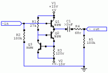
The circuit is designed for NPN transistors. Transistors which I have are PNP. I do not know how to change the circuit to accomodate my transistors. Would swaping power supply rails be enough?
Thanks for the help.
I would like to try nos germanium transistors in simple three-transistor buffer designed by Andrew Rothwell and shown on Nuuk's website: http://myweb.tiscali.co.uk/nuukspot/decdun/gainclonepre.html
The circuit is designed for NPN transistors. Transistors which I have are PNP. I do not know how to change the circuit to accomodate my transistors. Would swaping power supply rails be enough?
Thanks for the help.
This amplifier is designed for silicon transistors and would not work with germanium even if you reversed the supplies, as the bias would be different. What type of germanium transistors are you hoping to use as I may have a suitable preamp circuit?
Tony.
Tony.
Hello Tony,
Thanks for the response. I have 6 NOS TG52 transistors. This is a link to the datasheet. I have tried to attach it to this post, but the file is too big.
http://www.datasheetcatalog.com/datasheets_pdf/T/G/5/0/TG50.shtml
People who built this circuit complemented its sound quality. I have recently heared few germanium amps and I liked the sound very much. Is it possible to change the circuit to accomodate TG52 transistors?
I am a beginner in circuit design. I do not know how to do that.
Tom
Hi Tom
It appears to me this circuit is just a follower biased by a 2 transistor CCS. Vbe for a silicon BJT is 0.6V. When enough current flows through Q1 and Q2 to establish 0.6V on R3, Q3 turns on more, turning off more Q2 so that a constant current flows in Q1 and Q2. A form of negative feedback. In this case, 0.6V/120Ohms is 5mA. For a germainium transistor, Vbe is 0.3V instead of 0.6V as for silicon. So if you wanted the circuit to bias with germainuim parts at 5mA, you would have to change R3 to 60 Ohms. Obvioulsly since you have PNP instead of NPN ploarity transistors, the rail polarity should be reversed as well. I don't see why it wouldn't work the same otherwise.
It appears to me this circuit is just a follower biased by a 2 transistor CCS. Vbe for a silicon BJT is 0.6V. When enough current flows through Q1 and Q2 to establish 0.6V on R3, Q3 turns on more, turning off more Q2 so that a constant current flows in Q1 and Q2. A form of negative feedback. In this case, 0.6V/120Ohms is 5mA. For a germainium transistor, Vbe is 0.3V instead of 0.6V as for silicon. So if you wanted the circuit to bias with germainuim parts at 5mA, you would have to change R3 to 60 Ohms. Obvioulsly since you have PNP instead of NPN ploarity transistors, the rail polarity should be reversed as well. I don't see why it wouldn't work the same otherwise.
Attachments
Hi,
Q2 & 3 are a Constant Current Sink (CCS), there is little difference in changing to a germanium based version, except that germanium is not as temperature stable and the CCS current may turn out to be not very constant.
Q1 is the amplifier, operating in emitter follower (EF) mode. Sometimes known as common collector amplifier.
The characteristic of EF is high input impedance and low output impedance. Gain is almost 1 (+0db). It makes a nice unity gain buffer.
As per CBS240's recommendations...
Does this be do it?
Does this be do it?
An externally hosted image should be here but it was not working when we last tested it.
Yep, but I would also go for a smaller R2, this will help against noise. Unless you are using a fet, BJT's like a more moderate source impeadance. Actually, this resistor should be matched to the output impeadance of the signal source.
I don't think so.CBS240 said:Yep, but I would also go for a smaller R2, this will help against noise. Unless you are using a fet, BJT's like a more moderate source impeadance. Actually, this resistor should be matched to the output impeadance of the signal source.
Connect a low source impedance to the input.
Now look at the impedance of that input line to ground. It is Rs//Zin. The effect of Zin is almost unmeasurable with respect to tolerance to interference.
If a 20k pot preceeds the buffer then worst case Rs//Zin on the buffer input is 5k5//100k=5k2.
As is usual for all high Rs sources the leads MUST be kept short and preferably screened. If that pot wiper feeds directly to the buffer input, interference susceptibility is not an issue.
I was thinking more in general terms. IMO, it is better to have the lowest Zin possible for whatever the given application. For a mic input, obviously it wouldn't be that small. The application detail in this thread is vague.
Hello,
Thank you for the responses. Tony, thanks for the e-mail. One of the posts refers to use of pot at the input. Actually, I thought about asking that question. Yes, I would like to use pot at the input. I see, that suggested value is 20k. Can I use 10k or 50K? I have few of those.
And the last question: is it possible to use this buffer as stand alone? I do not use long interconnects, the longest are half of the meter. What I understand, unity gain buffers "do not like" to drive higher impedance cables.
Thanks again,
Tom
Hi,TB said:....... Yes, I would like to use pot at the input. I see, that suggested value is 20k. Can I use 10k or 50K? ............is it possible to use this buffer as stand alone? I do not use long interconnects, the longest are half of the meter. What I understand, unity gain buffers "do not like" to drive higher impedance cables.
if you decide to buffer the pot then either value will do OK.
Similarly, the buffer with it's low output impedance allows long cables.
I don't understand your last statement. I suspect you've quoted it wrongly.
Characteristic impedance of cables only applies at higher frequencies than audio. eg, 75ohm coax or 110ohm twisted pair.
These characteristic impedances are completely irrelevant at analogue audio frequencies. They do become very important at radio frequencies (RF) and for digital which are in the Mb/S and supposed to be squarewave requiring a bandwidth at least 10times higher.
Hello AndrewT,
I have must misunderstood information given in other posts. Whenever bufer was mentioned, solid state or chip based, it was recommended to keep the buffer as close to the amplifier as possible ( the best in the same enclosure0. The same was stated by Pavel Macura in his chip based buffer circuit.
In this case, where are the weak points of buffers?
Hi,TB said:...Whenever bufer was mentioned, solid state or chip based, it was recommended to keep the buffer as close to the amplifier as possible ( the best in the same enclosure0. The same was stated by Pavel Macura in his chip based buffer circuit....
I can't see a reason for recommending as close as possible.
Hopefully Pavel will come in and explain.
If you were to omit the buffer and use a pot only then the complete opposite applies. The pot output must be very close to the next stage AND the next stage must be designed to tolerate the variable source impedance.
- Status
- Not open for further replies.
- Home
- Amplifiers
- Chip Amps
- Use of PNP transistors instead of NPN in buffer circuit.