What can I say, I'm somewhat obsessive - I ran a sim on a version of a MOSFET A40 with mos ins & outs and bipolar VAS and input bias. I biased the input stage at ~ 5ma/side, with output bias current similar to the original A40 outputs, but with 2 X IRFP140 and IRFP9140 for outputs. I get about 0.02% THD with mostly 2nd harmonic and a nice distribution of higher order harmonics This is not a terrible place to be, but still more than the original bipolar/Darlington incarnation of the A40, at least according to sims. So, if sims prove out, you won't have ultimate bragging rights for THD, but still a nice-sounding amp if the simmed distortion profile is similar to what the actual amp will deliver. I'll look at this first-off sim a bit more when I get back from my business trip.
This may not be all that surprising, as the mos devices will have lower transconductance than bipolars at similar bias points.
Would there be a distortion advantage by using output FETs with better matched transconductance than the IRFP140/IRFP9140? Like the IRFP240/IRFP9140 for example?
It looks like C2 should be turned around. You see, this is why I'm doing the update, to be able to replace the pesky electrolytics/tantalums with film caps. I'm definitely using a cap at the input in my new design, as amps that pass DC all the way through give me the creeps - a disaster waiting to happen...
Dunno about any difference output mosfet substitution would make - if the models are generic, it won't show up in the sim.
The original circuit doesn't do much more than .01 to .04 % distortion @ THD1Would there be a distortion advantage by using output FETs with better matched transconductance than the IRFP140/IRFP9140? Like the IRFP240/IRFP9140 for example?
So no it would not do anything beneficial as far as the numbers game
The mosfets are just very easy to drive and eliminate the need for darlingtons.
Otherwise the main benefit is something with higher Safe Operating Area
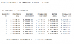
I just actually tried the simulation again in the version of PSpice I have here at work, with IRFP240 and IRFP9140 - I'm still getting around 0.02% distortion. Again, when I get back from my work trip, I'll probably try pumping up the current in the input diff stage using my supplemental current source trick to see if I can push down the THD that way - more parts, but maybe worth the trouble.
Boky - it will be non-polar in the new circuit - It'll be film. If everyone wants to try the bipolar version, a bipolar electrolytic may be an option, but there will likely be a size penalty. I think I'd trust the cap orientation that NP had in the original circuit.

2ma should be good for diff current.I just actually tried the simulation again in the version of PSpice I have here at work, with IRFP240 and IRFP9140 - I'm still getting around 0.02% distortion. Again, when I get back from my work trip, I'll probably try pumping up the current in the input diff stage using my supplemental current source trick to see if I can push down the THD that way - more parts, but maybe worth the trouble.
Blasting current into the diff can maybe improve slew rate. But for the most part
if using a mirror. It is just asking for stability problems in the real world.
It might be somewhat helpful if using FET input in simulation. But again real world
I would likely cascode the FET at lower voltages around 7 to 15 volts. And actually take advantage
of the purpose which is low noise / high impedance input.
In simulation its very unlikely the FET's will get lower distortion numbers. In real life more helpful for noise
reduction.
With a Simple Current mirror for the diff pair , and then adding the Darlington to the 2nd Gain stage/ Vas
You should easily get down to .004 % to .001 % distortion
adding the Darlington should be able to half the compensation cap needed.
of course the mirror needs basic dropping resistors to stay balanced and be effective.
and we really dont need much more than a 50mV drop across the resistors for them to be effective.
Since tail current is 2ma and each leg is at 1ma then it is dirt simple to figure the drop.
56 ohms will drop 56 mV and basically be as good as it gets.
by adding the mirror and improving the Vas I got it down to .004%
It depends on whether you want to preserve the simple VAS approach that NP used, or to go no hold barred and use all the latest tricks. I still intend to use either nmos or njfet for the input diff stage - thos will need a little more current to properly light them up.
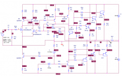
I just did a schematic with fairly limited bias current in the nmos input stage, with current mirror loading of the input diff stage and and Darlington config on the upper VAS stage - I got around 0.005% THD in sim, with good harmonic distribution. The design will work rather well if you throw a few more parts at it. This was also with a MOS output stage. I used NP's trick of bypassing the output stage with the compensation. The first attempt oscillated (even in sim) without that extra touch. I'll probably keep pecking away at this thing while I'm gone on my business trip...
Last edited:
It goes both way I think.
Getting more zeros behind the decimal point and being impressed.
Then running up against stability problems with those impressive zeros.
Or buying a bucket of parts to assemble. And realize sometimes it is similar romance
that tube guys have. Sometimes the components just look cool and are fun to look at.
Big metal cans, or cool looking big heatsinks.
Long as it makes you happy, it is all that matters.
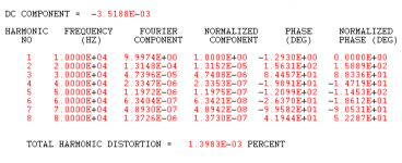
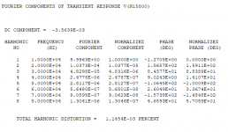
OK, I got a chance to run a sim on my updated version of the A40 mosfet design, mixing mos and bipolar. Running up the tail current on the mos input stage to 10ma/side (higher transconductance) pushed the THD down to 0.004% with low odd-order components. I think I have a little more room to tweak this design, as the offset in the sim is around 1.7 mV. I have found in practice (at least in sims) that the closer I can balance the input stage in terms of static bias, the lower the THD. So, now that I'm back in the US (as of last night, late) I have access to faster sims, and can sharpen my pencil on this design. A provision for adjusting the static bias to balance the input stage is definitely in order.
My current version of this sim uses the Zetex/Diodes, Inc. super bipolar devices, which are currently unobtainium ( a huge lead time) via the top two catalog distributors. I will be replacing the bipolars with 2N5401 and 2N5551 as appropriate - this will change the static bias points slightly.
My current version of this sim uses the Zetex/Diodes, Inc. super bipolar devices, which are currently unobtainium ( a huge lead time) via the top two catalog distributors. I will be replacing the bipolars with 2N5401 and 2N5551 as appropriate - this will change the static bias points slightly.
Last edited:
One way to adjust bias might be this.
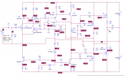
Install resistor R991 matched to resistor R87. Change fixed resistor R12 to 100 ohm trimpot (25 turns).
Twirl the knob on trimmer R12 until the voltage at test point TP-1 exactly equals the voltage at test point TP-2. On the "IPS6" daughter card, this was straightforward to do: just connect the DVM probes to TP-1 and TP-2, then trim until the voltage difference is zero. (link to IPS6 schematic in post #3,408).
_
Attachments
Last edited:
Both simulations are using the original A40 compensation scheme which closes the loop at the VAS without including the output stage.
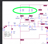
I am running a fairly large current in the mosfet input stage to boost open loop gain. Attached is another version that uses higher value resistors on the current mirror - the output offset isn't as nice, but the THD in simulation is still very low.
Attachments

Often designers choose emitter degeneration resistors in current mirrors, so that the voltage dropped across each emitter resistor, is MANY times larger than the maximum expected Vbe mismatch between the mirror devices (Q3 and Q4). Thus if it is expected that Q3 and Q4 can have Vbe's which differ by 10 millivolts, arrange for their emitter resistors to drop 150 millivolts; a factor of 15X greater than delta-Vbe. Now, even with mismatched transistors, the current mirroring ratio (Iout / Iin) remains very close to 1.000. This can be explored in simulation, simply by installing a ±10 millivolt independent voltage source in series between Q4_base and the rest of the circuit.
- Home
- Amplifiers
- Pass Labs
- Updated Pass A40 Design