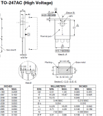
That might be an option if you come across some of the older Motorola/onsemi TIP142 and TIP147 still in the original TO-3P package. Newer parts are all TO-247 these days.
Back to post #5 - I checked out the data sheet for the New Jersey Semiconductor version of the Lambda Darlingtons - I found it somewhat disturbing that they don't state the values for the bias resistors. I wouldn't be too surprised if the values are a lot higher, as that would be an easier option for the fab.
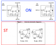
As an example, here's what ST did to the bias resistors in the 2N6283 series:
https://www.mouser.com/datasheet/2/389/CD00001223-491041.pdf
Compare that to the values in the onsemi part.
As an example, here's what ST did to the bias resistors in the 2N6283 series:
https://www.mouser.com/datasheet/2/389/CD00001223-491041.pdf
Compare that to the values in the onsemi part.
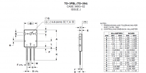
I have some actual onsemi TIP142G and 147G parts - I'll be checking the mounting holes. I remember getting some TIP142 Darlingtons from Fairchild a few years back (before the merger) that were in some funky derivative of a TO-3P package that took a 3mm mounting screw rather than a #6 like in the case of a legit TO-247. The original TO-3P parts had an exposed drain tab that would have taken a TO-3 insulating bushing and a #6 screw. They were actually made as cheap stand-ins for a TO-3 device, and meant to fit over the std TO-3 hole pattern with the tab lined up over one of the mounting holes and the base and emitter leads bent and poking down through their respective holes . The exposed tab evolved over the years, starting out with a shape similar to the TO-3 package and ending up squareish.
Last edited:
Here is the onsemi data sheet for the TIP142G/147G - the device with the exposed metal tab is what passed for a TO-3P. After June 2012, the device was only manufactured in the TO-247 package.
https://www.onsemi.com/download/data-sheet/pdf/tip140-d.pdf
The original TO-3P package looked like what is shown in the old TI spec for the TIP140 series::
http://pdf.datasheetcatalog.com/datasheet_pdf/texas-instruments/TIP130_to_TIP142.pdf
https://www.onsemi.com/download/data-sheet/pdf/tip140-d.pdf
The original TO-3P package looked like what is shown in the old TI spec for the TIP140 series::
http://pdf.datasheetcatalog.com/datasheet_pdf/texas-instruments/TIP130_to_TIP142.pdf
Last edited:
The package was actually a TO-218 variant, but it was informally called a TO-3P due to its original purpose as a cheap sub for the TO-3 metal package. The Asian take on TO-3P is an entirely different matter.
Back to post #5 - I checked out the data sheet for the New Jersey Semiconductor version of the Lambda Darlingtons - I found it somewhat disturbing that they don't state the values for the bias resistors. I wouldn't be too surprised if the values are a lot higher, as that would be an easier option for the fab.
As an example, here's what ST did to the bias resistors in the 2N6283 series:
https://www.mouser.com/datasheet/2/389/CD00001223-491041.pdf
Compare that to the values in the onsemi part.
On Semi and ST both use 8k and 60 ohms.
Ironically both data Sheets have errors.
OnSemi= shows 50 ohm in the test data graph, then shows 60 ohms in the schematic.
ST = shows a print error instead of reading 60 ohms they printed 60k
Attachments
awesome, thanks! I picked up a bunch of MJH6284/87, gonna give those a try, they seem a bit more stout than the TIP142/47. Made some boards for the TO247 style outputs, so I'll be able to swap them out. And I def will try out the 'new' bipolar front end first, and I'm highly intrigued by the mos version. Appreciate the effort. If it doesnt blow up and sounds decent, what more can you ask for!
john
john
There you go.
Very nice, it is a fun amp.
That is more like the original.
Basically the magic.
the simple 2nd gain stage with no beta enchantment
is basically what gives the amp the slight rise in 2nd harmonic.
Amplifier isnt AC coupled so you get 35 to 40 mv
of DC offset on the output.
Q7 could of always had a current limit emitter resistor.
if you just add the usual 22 to 27 ohm emitter resistor
DC offset will drop to around 5 to 7 mv
instead of 35 to 40
or just add input cap and get around the same.
be warned the magical 2 nd harmonic goes away with emitter resistor.
add slower 2nd gain transistor or add something with
less gain. and the magic erupts.
or just remove the transistor CCS
and go old school with a bootstrap.
if you want even less third harmonic.
bias at class B
add slower 2nd gain transistor or add something with
less gain. and the magic erupts.
or just remove the transistor CCS
and go old school with a bootstrap.
if you want even less third harmonic.
bias at class B
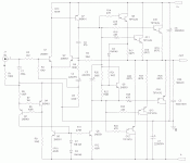
MikeW posted an all mosfet 'A40' years ago on this forum, i'll have to dig in the archives for the schem, I believe he used the 240/9240.
found it, schem at the top:
https://www.diyaudio.com/community/threads/mosfet-a40.52104/
found it, schem at the top:
https://www.diyaudio.com/community/threads/mosfet-a40.52104/
Last edited:
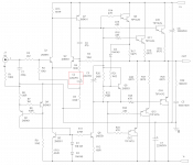
I will lay out the board to take 3 X TO-247s per side. If users want to use just two of the more robust devices per side, no complaints. Keep in mind also that you can string leads from the TO-247 holes for TO-3 packages. For just 2 devices, you probably want to use 0.68 ohm emitter resistor like the original, and the resistors around the bias transistor will also change a bit, as you will need to run more current per device.
I will be gone for international business travel starting Thursday for ~10 days, so don't get frosted if you see no activity from me on this front. I still have two modified Hitachi-type lateral mosfet amp boards at home that are begging for completion. This will involve matching up the input pmos stage and selecting the laterals for the output. Once I get a sense of the required Vgs for the laterals, I can appropriately adjust the bias resistors.
Just for grins, I had a look at the A40 mosfet schematic. With an all- mosfet design, selection of devices would be a definite pain, esp. for the VAS stage. I would want to use some lower capacitance devices for the input diff stage, and depletion-mode biasing for the input diff stage. I may make some passes at that design sometime in the future, but my plate is overflowing at present...
It may be more straightforward to mix bipolar and mosfet in the design. - keep the mosfet inputs and outputs, and the Vgs multiplier, but maybe use bipolars for the VAS and perhaps add a follower stage to drive the output mosfets. Lateral output devices (more of them) might be a better choice in terms of thermal stability and input capacitance. These are just initial musings at present.
It may be more straightforward to mix bipolar and mosfet in the design. - keep the mosfet inputs and outputs, and the Vgs multiplier, but maybe use bipolars for the VAS and perhaps add a follower stage to drive the output mosfets. Lateral output devices (more of them) might be a better choice in terms of thermal stability and input capacitance. These are just initial musings at present.
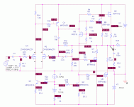
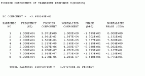
What can I say, I'm somewhat obsessive - I ran a sim on a version of a MOSFET A40 with mos ins & outs and bipolar VAS and input bias. I biased the input stage at ~ 5ma/side, with output bias current similar to the original A40 outputs, but with 2 X IRFP140 and IRFP9140 for outputs. I get about 0.02% THD with mostly 2nd harmonic and a nice distribution of higher order harmonics This is not a terrible place to be, but still more than the original bipolar/Darlington incarnation of the A40, at least according to sims. So, if sims prove out, you won't have ultimate bragging rights for THD, but still a nice-sounding amp if the simmed distortion profile is similar to what the actual amp will deliver. I'll look at this first-off sim a bit more when I get back from my business trip.
This may not be all that surprising, as the mos devices will have lower transconductance than bipolars at similar bias points.
This may not be all that surprising, as the mos devices will have lower transconductance than bipolars at similar bias points.
Attachments
Last edited:
I may end up using the same supplemental bias scheme that I used in my earlier design to push down the distortion. The combination of mos and bipolar should result in an amp that's easier to build.
- Home
- Amplifiers
- Pass Labs
- Updated Pass A40 Design