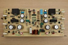
For a while, I’ve been stuck on repairing a channel of my Accuphase P-266. Initially, I tracked the fault to a shorted dual transistor (Q3: uPA75V) in the complementary differential input stage. I replaced both dual transistors with matched KSC1845 and KSA992 transistors. Additionally, I discovered that the R23 68-ohm fusible resistor was open, so I replaced it with a regular metal film resistor.
When I turned the amplifier on, nothing seemed out of the ordinary. However, when I began measuring the bias on T.P.1, I noticed the reading was very unstable. According to the schematic, the correct reading for T.P.1 in class AB mode is 88mV, but the value fluctuated wildly. It would jump well above 100mV and sometimes drop all the way down to 14mV.
I tested all the semiconductors in diode mode with my multimeter and didn’t find any anomalies. I’ve also replaced all the electrolytic capacitors. At this point, I’m stumped and unsure of what could be causing the issue.
Here are a few possibilities I’m considering:
I’ve attached a photo of the repaired board for reference. I would appreciate any insights or advice!
When I turned the amplifier on, nothing seemed out of the ordinary. However, when I began measuring the bias on T.P.1, I noticed the reading was very unstable. According to the schematic, the correct reading for T.P.1 in class AB mode is 88mV, but the value fluctuated wildly. It would jump well above 100mV and sometimes drop all the way down to 14mV.
I tested all the semiconductors in diode mode with my multimeter and didn’t find any anomalies. I’ve also replaced all the electrolytic capacitors. At this point, I’m stumped and unsure of what could be causing the issue.
Here are a few possibilities I’m considering:
- Could the trimmpotentiometers be faulty? I’ve cleaned them with IPA and lubricated them with contact cleaner, but could they still be causing the instability?
- Could the new complementary differential input transistors I installed be contributing to the problem?
- Is it possible that a diode or a transistor, while testing well, is failing under load?
I’ve attached a photo of the repaired board for reference. I would appreciate any insights or advice!
Attachments
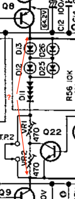
Not a lot to cause that problem, a few diodes and a transistor, that's all.
Q22 is normally switched on when in class B and switches off in class A. That eliminates VR2 so just VR1 and the diodes.
Monitor the voltage across D11 ... does it vary ... if it does, it is faulty.
Do the same with D12, 13, 25 & 26.
If all OK then that leaves just Q22, monitor its CE voltage.
Ensure they are thermally in contact with the power output heat sink, if appropriate.
Thanks for the response!
I went ahead and made some measurements. When I powered on the amp, the readings on T.P.1 started around 60mV and immediately began to drop.
While the readings on T.P.1 were decreasing, I checked the voltage drops across the following components with my second meter, and they all seemed stable:
The voltage across the CE on Q22 was also stable, reading around 70mV.
Interestingly, I noticed that when I turned off the amp, the readings on T.P.1 actually started going back up for a brief moment.
I went ahead and made some measurements. When I powered on the amp, the readings on T.P.1 started around 60mV and immediately began to drop.
While the readings on T.P.1 were decreasing, I checked the voltage drops across the following components with my second meter, and they all seemed stable:
- D11: 2.4V
- D12, D13, D25, D26: 1.9V
The voltage across the CE on Q22 was also stable, reading around 70mV.
Interestingly, I noticed that when I turned off the amp, the readings on T.P.1 actually started going back up for a brief moment.
I believe you may have looked at the T.P.2 instead of T.P.1. The bias adjustment is done across the R63 resistor. The voltage across this resistor starts immediately dropping after powering on the amp. It is unclear why.Not a lot to cause that problem, a few diodes and a transistor, that's all.
Q22 is normally switched on when in class B and switches off in class A. That eliminates VR2 so just VR1 and the diodes.
Monitor the voltage across D11 ... does it vary ... if it does, it is faulty.
Do the same with D12, 13, 25 & 26.
If all OK then that leaves just Q22, monitor its CE voltage.
Ensure they are thermally in contact with the power output heat sink, if appropriate.
The bias current is measured across R63. Not set by.
The bias is set with the diodes combination as I explained and if any of the diodes vary, that will vary the bias current.
The bias current is set by a combination of VR1 and VR2.
Hence to accertain that there is no instability with the voltage set between the collectors of Q8 and Q9.
The bias is set with the diodes combination as I explained and if any of the diodes vary, that will vary the bias current.
The bias current is set by a combination of VR1 and VR2.
Hence to accertain that there is no instability with the voltage set between the collectors of Q8 and Q9.
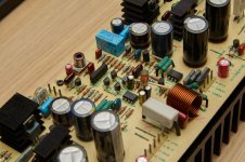
Attachments

@Vunce
Unfortunately, I haven’t resolved the issue yet. Between time constraints and a few knowledge gaps, I had to put the repair on hold for a while. That said, I’m planning to get back into it soon and hopefully restore this beautiful amp to its former glory.
Unfortunately, I haven’t resolved the issue yet. Between time constraints and a few knowledge gaps, I had to put the repair on hold for a while. That said, I’m planning to get back into it soon and hopefully restore this beautiful amp to its former glory.
I’ve tried a several times to translate those written remarks with a translator app and still don’t have a solid translation.
If you know what the comments say, please post here in English.
Thank you.
If you know what the comments say, please post here in English.
Thank you.
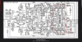
I have to admit that I did the schematic scan and wrote the remarks, but repairs like this are long time ago and I have no memory of additional details.
...
Translation of the remarks from left to right :
Start up problem : D11 has no current
Start up problem, bias circuit no current : have a look at Q8, Q9 even if they seem to be OK
(+) Attention, cut three copper traces connecting the sources of power transistors.
Check solder connections of all power transistors
This schematic is similar to the power amp stage of E-303
And on top : Replacement of output devices with J200 and K1529 requires short out of D13 to adapt the bias. VR1 and VR2 have the correct rotational orientation.
...
The schematic and print layout have a serious design error :
If you have a close look at the diagram, sources of n and p channel output pairs Q12/Q13, Q14/Q15 and Q16/Q17 are connected with a respective copper trace. This way the function of source resistors R34 .. R39 is impaired.
These three traces have to be cut without disconnecting the base resistors R41 .. R46 of the current limit transistors Q20 and Q21.
I remember these three traces went all along the large side of the board from left to right to the transistor mounting sides, and this was the point where I cut the copper, but it should be checked.
I did this modification to both channels of all P-266 repair units to improve bias stability.
...
Translation of the remarks from left to right :
Start up problem : D11 has no current
Start up problem, bias circuit no current : have a look at Q8, Q9 even if they seem to be OK
(+) Attention, cut three copper traces connecting the sources of power transistors.
Check solder connections of all power transistors
This schematic is similar to the power amp stage of E-303
And on top : Replacement of output devices with J200 and K1529 requires short out of D13 to adapt the bias. VR1 and VR2 have the correct rotational orientation.
...
The schematic and print layout have a serious design error :
If you have a close look at the diagram, sources of n and p channel output pairs Q12/Q13, Q14/Q15 and Q16/Q17 are connected with a respective copper trace. This way the function of source resistors R34 .. R39 is impaired.
These three traces have to be cut without disconnecting the base resistors R41 .. R46 of the current limit transistors Q20 and Q21.
I remember these three traces went all along the large side of the board from left to right to the transistor mounting sides, and this was the point where I cut the copper, but it should be checked.
I did this modification to both channels of all P-266 repair units to improve bias stability.
Ahhh...
From the few P-266 amps needing repair I've read about on the Web, the output transistors were taken out. This design issue you bring up might be a main cause for the damage. I have one of these amps on the way to me and will definitely check this out.
I'll check out the Amp8 Accuphase P-266 restoration and see if he addresses this also.
Thank you for clearing up the schematic remarks and this additional information, as_audio!

Edit:
Referring to the annotated attached image.....
Would these be the correct locations to cut the Source traces and still keep the 680R base resistors for Q20/21 intact?
From the few P-266 amps needing repair I've read about on the Web, the output transistors were taken out. This design issue you bring up might be a main cause for the damage. I have one of these amps on the way to me and will definitely check this out.
I'll check out the Amp8 Accuphase P-266 restoration and see if he addresses this also.
Thank you for clearing up the schematic remarks and this additional information, as_audio!
Edit:
Referring to the annotated attached image.....
Would these be the correct locations to cut the Source traces and still keep the 680R base resistors for Q20/21 intact?
Attachments
Last edited:
Sorry for the slang term, "taken out" does mean burnt out, kaput, Poof!! 🤣
Amp8.com link for P-266 repair:
http://amp8.com/tr-amp/accuphase/p-266.htm
Amp8.com link for P-266 repair:
http://amp8.com/tr-amp/accuphase/p-266.htm
In this link you can see pictures of the pcb, copper side.
The three traces that should be cut are easily visible on a long side of the board.
The three traces that should be cut are easily visible on a long side of the board.
Last edited:
Yes, I clearly see the source connection traces in question. 👍
I'll check the E-303X schematic also, this unit was build during the same years as P-266 with similar output stage MosFet's.
I'll check the E-303X schematic also, this unit was build during the same years as P-266 with similar output stage MosFet's.
My suggestion may apply to model E-303 also, but it is not completely clear from my handwritten remarks. Where is the 303 schematic that you use ?
In the schematic of post 1 here (I do not know it is original) :
it seems Accuphase did it in the correct way.
In the schematic of post 1 here (I do not know it is original) :
I have a DC-offset issue on one channel of an Accuphase E-303, and I can't seem to find the cause, so I could really use some help.
Starting point:
All electrolytics are new.
All other components have been measured and checked (several times).
I found only one defective diode: D3.
It works and plays music just fine, and THD is normal.
BUT: As the amp warms up, the right channel drifts from DC offset at basically zero, to about 650-700mV (a rather suspicious value..).
The left channel only drifts around 30mV, which seems normal/reasonable.
Initially I suspected the input stage, but it...
The E-303 used Hitachi TO-3 Lateral MosFet's and is much different than the amplifier section of E-303X which uses Toshiba K405/J115.
The E-303X shares very similar circuit as P-266.
303X also has the complementary MosFet source pins connected like P-266
The E-303X shares very similar circuit as P-266.
303X also has the complementary MosFet source pins connected like P-266
Attachments
Yes, reading my badly written remarks in the P-266 diagram it seems I confused E-303 and E-303X in post 11 and consequently in post 17.
The respective remark should read This schematic is similar to the power amp stage of E-303X in post 11.
Having a look at your E-303X schematic of post 18 it is completely crazy, because the output source resistors are bridged (but the connection to the current limit transistors is correct). Still we have to compare the pcb layout. I am waiting for the experts explaining us this is no design error.
Your scan of the 303X schematic is better than mine but it has the adjustment instructions.
Acuphase E-303X diagram, adjustments
..
..
Last edited:
- Home
- Amplifiers
- Solid State
- Unstable Bias on Accuphase P-266: Need Help Diagnosing