design idea to use UJ3N065080K3S PowerJFET.
Kokorian shared his SRPP design concept to me. He gave the following information:
"The lower jfet adjusts the quiescent output voltage, the upper, the bias current. The P jfet keeps the voltage of R1 +R2 constant, by this it modulates the upper jfet current inversely to that of the lower. All values are to be considered as demo."
I
Attachments


0.5 + 0.5 ohms would be nice... With a UF3N-series JFET I can't seem to take it much below 3 + 3 ohm. And with a low rail voltage, I lose almost 8V across those resistors. The distortion is very low, but it's an unwieldy class-A monster, with bonus 9V coin cells to allow the VAS to drive the lower JFET.
But I think I might build one... I accidentally left a source resistor in that was eating away even more voltage, but an 8V drop isn't that bad, given that I'd already been considering a single-ended option with a pull-up resistor and small inductor.
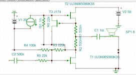
I have a version that I've been playing around with on TINA. Try R1 = R2 = 3.0 ohm. I tried with 0.5 ohm but it seems like wishful thinking.
Vgs (Multimeter #6) was around -7 to -9V. My simple brain says to use coin cells for the DC offset connecting to a VAS, although I'd have to double check there's no trickle charging going on.
Vgs (Multimeter #6) was around -7 to -9V. My simple brain says to use coin cells for the DC offset connecting to a VAS, although I'd have to double check there's no trickle charging going on.
It looks like Q4 and Q5 are attached to the output through a multimeter
This version uses 9V to generate a negative voltage, and without local feedback. Notice that a negative supply is not needed for the upper JFET because of the almost 8V drop across R1 and R5 (ouch!). The overly-complicated NFB changes from voltage feedback in the bass, to current feedback at high frequencies, which makes the EQ a bit wonky if connected to a real speaker. The speaker model is a bit exaggerated, though, because it doesn't take into account decreasing L at HF.
It can be simplified by running just the V-feedback, but I think it would be a waste to use the SRPP topology that way, since we've already gone to the trouble of converting an input voltage to an output current. There are lots of proven push-pull MOSFET designs with the N-channel on top.
Hi Abstract... thanks for sharing your ideas. This is SRPP+?
Only 1V out in 8 ohm? I see you are using different FETS. Did you get the model for uj3n065080k3s working in TINA? Kokorian couldn't get the model working in TINA.
Only 1V out in 8 ohm?
I see you are using different FETS. Did you get the model for uj3n065080k3s working in TINA? Kokorian couldn't get the model working in TINA.The input was 200mV for a gain of about 5, and should be good for +/-5 or so Vout before encountering clipping or instability.
The JFET 'floating' CCS could probably be refined into something more like an Aleph or resembling a push-pull system so it doesn't draw so much idle current. But it's not exactly obvious to me without resorting to actual push-pull.
The JFET 'floating' CCS could probably be refined into something more like an Aleph or resembling a push-pull system so it doesn't draw so much idle current. But it's not exactly obvious to me without resorting to actual push-pull.
- Home
- Amplifiers
- Solid State
- UnitedSIC UJ3N065080K3S SIC FET Amplifier Design Idea