After the power keys in the power supply burn out, most often there are malfunctions in the key control circuit.

It is very important that the capacity of the capacitor C13 is stable. Diodes D10 D11 often break down, they are also important, transistors Q3 Q4 also break down and sometimes transistors inside TL494 break down. If diodes D10 D11 are broken down or the capacity of capacitor C13 is low, then the miracles that you see will also happen.

C7 C8 D7 D8 and also create the miracles that you observe.
It is very important that the capacity of the capacitor C13 is stable. Diodes D10 D11 often break down, they are also important, transistors Q3 Q4 also break down and sometimes transistors inside TL494 break down. If diodes D10 D11 are broken down or the capacity of capacitor C13 is low, then the miracles that you see will also happen.
C7 C8 D7 D8 and also create the miracles that you observe.
Last edited:
The most common reason for unstable operation of the power supply is unstable standby power. Most often, the capacitor dries out there.

Frankly, the inductor always heated up a lot, but it never caused the power supply to break.
I think should have more turns for 30V. Of course for this chinese PSU it is not calculated right.
Maybe now it lost permeability even at low temperature? I am going to change it with a new identical one and see if it works.
If it actually solves the problem, i will later change it with another inductor with MORE turns. The core always dissipated a lot of power and always heated up a lot.
So maybe now it completely lost permeability even at room temperature.
It is a possibility.
All the diodes are perfectly ok.After the power keys in the power supply burn out, most often there are malfunctions in the key control circuit.
View attachment 1341297
It is very important that the capacity of the capacitor C13 is stable. Diodes D10 D11 often break down, they are also important, transistors Q3 Q4 also break down and sometimes transistors inside TL494 break down. If diodes D10 D11 are broken down or the capacity of capacitor C13 is low, then the miracles that you see will also happen.
View attachment 1341310
C7 C8 D7 D8 and also create the miracles that you observe.
The capacitors also seem ok.
I will try to change the tl494 as well.
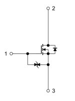
That would be for excess gate/source voltage protection. If the drive voltage is below the FET's G/S breakdown limits it shouldn't be an issue but I think you did mention transformer coupling for the gates... that could throw up some surprises so again you need to scope the drive to see what the amplitude and quality is like.
Remember the primary side will not be isolated from the mains so that makes using a scope more difficult unless you use isolation transformers.
Remember the primary side will not be isolated from the mains so that makes using a scope more difficult unless you use isolation transformers.
I can easily cheat this by using the pure sine wave inverter, but the problem is that i dont have an oscilloscope in the first place... Yes, i know, its a REAL PAIN.
Now, i just recieved every new component.
All the SMD transistors, SMD capacitors and SMD ICs are going to be replaced with new ones.
If it still doesn't work, i will look at the gate drive transformer and at the main transformer to find if they have a problem internally.
Now, i just recieved every new component.
All the SMD transistors, SMD capacitors and SMD ICs are going to be replaced with new ones.
If it still doesn't work, i will look at the gate drive transformer and at the main transformer to find if they have a problem internally.
- Home
- Amplifiers
- Power Supplies
- UNFIXABLE power supply!!?