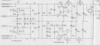
After a restoration of caps, res, diodes and tran my regulator i get uneven voltages. Should be +/- 82v but i get 81.4 and 84.0V.
Have used very tight tolerances on resistors, zeners etc, and Everything is double checked. Same as schematic except R713 wasn’t 1.8M but 1.2M ( not sure what does that resistor do)
A1830/C4793 is new old stock i had (not fake) and the other 2 are now ksc2690/a1220 (here i have 17.7 and 17.9v) so it seems to work better.
Any ideas why its like this and does it matter on the +/-82v reg?
Hfe was quite uneven on the 1830/4793 pair, would that be the case? 150 for 1830 and 270 for 4793. Checked all my 20-30 pieces i got and all where the same about so..
Attachments
That resistor network is part of the feedback and so value changes there will affect the regulated output voltage. The parallel resistor has been added for a reason but only the designer of the circuitry it feeds will know why.
The 18 volt supplies are just simple series pass elements where the output voltage is approximately the Zener voltage less the Vbe of the transistor. You will get slightly different voltages with different parts.
The 18 volt supplies are just simple series pass elements where the output voltage is approximately the Zener voltage less the Vbe of the transistor. You will get slightly different voltages with different parts.
That resistor network is part of the feedback and so value changes there will affect the regulated output voltage. The parallel resistor has been added for a reason but only the designer of the circuitry it feeds will know why.
The 18 volt supplies are just simple series pass elements where the output voltage is approximately the Zener voltage less the Vbe of the transistor. You will get slightly different voltages with different parts.
Ok i understand.
Just wonder if i can somehow adjust some resistor or other component so i can get it back to +/-82v. Does the Hfe affect the output a lot?
You could substitute R718 with a combination of a 30k resistor and 5k pot in series to make it adjustable…
Hfe shouldn't really affect things at all tbh. The positive output mirrors the negative with the negative being the 'reference' which it tracks and follows. If the negative rail changes the positive one will mirror that change.
Designs like this are not intended for absolute precision in terms of voltage output. The three Zeners set the basic reference voltage the negative rail works to and they have a pretty wide tolerance.
Precision doesn't matter in this application. The fact the designer has made the rails deliberately unbalanced has been done for a reason, the two most likely being that it prevents some undesired behaviour in the circuitry supplied by the regulators and/or it simply gives better performance on paper.
QUAD deliberately ran one of their preamps on unbalanced supplies with one rail a bit different to the other and the reason was that the unbalanced rails actually made the point at which the output clipped more symmetrical. So it just looked better when tested.
You could substitute R718 with a combination of a 30k resistor and 5k pot in series to make it adjustable…
Ohh well maybe i could try but space there is not much of, so what you’re saying is that i serieconnect a trimpot (0.5w bourns for example with 3 pins) say 5-10k or with an about 30k res?
Hfe shouldn't really affect things at all tbh. The positive output mirrors the negative with the negative being the 'reference' which it tracks and follows. If the negative rail changes the positive one will mirror that change.
Designs like this are not intended for absolute precision in terms of voltage output. The three Zeners set the basic reference voltage the negative rail works to and they have a pretty wide tolerance.
Precision doesn't matter in this application. The fact the designer has made the rails deliberately unbalanced has been done for a reason, the two most likely being that it prevents some undesired behaviour in the circuitry supplied by the regulators and/or it simply gives better performance on paper.
QUAD deliberately ran one of their preamps on unbalanced supplies with one rail a bit different to the other and the reason was that the unbalanced rails actually
made the point at which the output clipped more symmetrical. So it just looked better when tested.
When i replaced The zeners i choose 2% tolerance parts and 1.3w instead of 0.5w, i was just thinking lite overkill. Resistors are spot in, i had most of them as 0.1% vishay 0207 and some Dale Rn60. What i had in the box.
Original the curcuit had 5% carbonfilm parts (many of them widely out of spec) and if i remember correctly the 2x33k was 1% metalfilm.
I also ofcourse replaced the sc2240/a970 with original toshiba parts.
This regulator goes really hot and components and board have taken a hit for that over the years hence all components swap out.
I also upgraded the heatsinks with coppersheets to cool it further plus drilled a bunch of ventholes in the board.
Thanks, i didn’t know Quad did that. Interesting..
well, it sounds pretty darn good compared to what it was i have to say. But i have a feeling that having extra 2 volt to the junctions wasn’t What the designer intended. NAD in this case. Model is 218. Big beast.
Here is the QUAD. Although it uses opamps throughout the designer unbalanced the rails to make the final 'clipping point' look more symmetrical when tested.
So I would leave yours as it is intended to be.
Ok but i think in the schematic it says -/+82v right? So they mean it should be even?
Not seen this behaviour in any Nad before, perhaps 0.5v difference but thats it
That was your main mistake: a 1.3W zener has a slightly lower voltage for the same current.When i replaced The zeners i choose 2% tolerance parts and 1.3w instead of 0.5w, i was just thinking lite overkill.
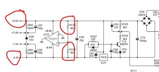
The role of the 1.8M resistor is to offset the effect of the error amplifier transistor's Vbe: the upper resistor sees a voltage of Vout-Vbe, and the lower one Vout+Vbe.
By lowering the correction resistor to 1.2M, you have over-corrected the circuit
That was your main mistake: a 1.3W zener has a slightly lower voltage for the same current.
The role of the 1.8M resistor is to offset the effect of the error amplifier transistor's Vbe: the upper resistor sees a voltage of Vout-Vbe, and the lower one Vout+Vbe.
By lowering the correction resistor to 1.2M, you have over-corrected the circuit
Ok thanks for clearing that out and i again learned something new. Well i have to replace those zeners then.
But in schematic it says 1.8M right but from factory it was 1.2M, i checked the original and the rings and it was 1.2M so replace with the same.
What would your suggestion be, try with 1.8M even though Nad went with 1.2M? They perhaps got a batch with slightly off spec transistors and did a “fix” in the production? Yea this 1.2M was clearly an orginal resistor, never replaced with factory soldering and same type as in rest of amp.That was your main mistake: a 1.3W zener has a slightly lower voltage for the same current.
The role of the 1.8M resistor is to offset the effect of the error amplifier transistor's Vbe: the upper resistor sees a voltage of Vout-Vbe, and the lower one Vout+Vbe.
By lowering the correction resistor to 1.2M, you have over-corrected the circuit
When i changed the transistors to a new batch this perhaps “upsetted” the curcuit?
You need to understand how the circuit works...
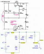
1/ The negative rail voltage rises because the two series pass transistors are turned hard on via R709 and R707.
2/ The Zeners conduct when their total volt drop rating is passed (so 27V * 3 = 81V).
3/ At this point TR706 begins to turn on because it gets its base current via the Zeners.
4/ As it turns on it begins to pull down the base of Q704 thus limiting any further rise in voltage.
So that's the negative rail. The output voltage approximately equals the Zener value.
5/ The positive rail is similar, the pass transistors are turned hard on.
6/ When the voltage on the base of Q705 starts to reach around 0.6V the transistor turns on thus limiting the positive rail voltage.
7/ The point it turns on depends only on the divider network of R718 and R712+R713 that are in parallel.
8/ So if the negative rail is at -82 volts then the positive rail must also reach +82V in order to give around 0.7 volts at the base of Q705. That happens because of the parallel 1.8meg resistor.
It's all 'exactly non exact' because the actual voltages you see depend on several different parameters.
Without the 1.8 meg you would see around 83.5V positive and negative 82 volts... but it's all non exact because of different parameters in the parts. And ultimately it probably doesn't matter at all.
Yes, the positive output voltage is set by R718 / (R712//R713) divider.
I think, the positive and negative voltages will be about the same if we:
1) Find equal R718 and R712. It is easy to find two the same value (+-0.5% or better) with any multimeter.
2) Get rid of R713. The difference between voltages will be about 0.6-0.7 V (Q705 Vbe). It's nothing (I mean quite good) as for me. It's not aerospace technology (I hope?). The difference less then 1.0V is quite good.
If one resistor is a bit smaller value then other - then it means there is no need in R713 1.8M. Just use smaller one as R712 and the larger one as R718.
Last edited:
The voltages across R711 and R715 will reveal the base current of Q705 and Q704 - which by my calculations should be 10uA or less for 10A output current - if somethings wrong with one of the transistors the current gain will be less, so one of these base currents might then be anomolously high, which could affect the DC match.
If the current here is basically negligible the match is solely down to the resistor network.
If the circuit is oscillating somewhere this would also affect the DC conditions.
If the current here is basically negligible the match is solely down to the resistor network.
If the circuit is oscillating somewhere this would also affect the DC conditions.
You need to understand how the circuit works...
1/ The negative rail voltage rises because the two series pass transistors are turned hard on via R709 and R707.
2/ The Zeners conduct when their total volt drop rating is passed (so 27V * 3 = 81V).
3/ At this point TR706 begins to turn on because it gets its base current via the Zeners.
4/ As it turns on it begins to pull down the base of Q704 thus limiting any further rise in voltage.
So that's the negative rail. The output voltage approximately equals the Zener value.
5/ The positive rail is similar, the pass transistors are turned hard on.
6/ When the voltage on the base of Q705 starts to reach around 0.6V the transistor turns on thus limiting the positive rail voltage.
7/ The point it turns on depends only on the divider network of R718 and R712+R713 that are in parallel.
8/ So if the negative rail is at -82 volts then the positive rail must also reach +82V in order to give around 0.7 volts at the base of Q705. That happens because of the parallel 1.8meg resistor.
It's all 'exactly non exact' because the actual voltages you see depend on several different parameters.
Without the 1.8 meg you would see around 83.5V positive and negative 82 volts... but it's all non exact because of different parameters in the parts. And ultimately it probably doesn't matter at all.
I don’t understand (i’m just not smart enough hehe)
I do appreciate and i really like how you explain how it works. Now i have somw understanding.
The measured voltage was -81.5v and +84v
Nad have themself put 1.2M, should i then try with a higher value like schematic says on R713? It seems then that the plus voltage are running to high but if that suppose to fallow the negative rail im lost whats wrong. So the zenerx3 is ok!? I do not need to change from 1.3w down to 0.5w? I have here 81.5v.
Sorry i’m confused now what to do next.
The voltages across R711 and R715 will reveal the base current of Q705 and Q704 - which by my calculations should be 10uA or less for 10A output current - if somethings wrong with one of the transistors the current gain will be less, so one of these base currents might then be anomolously high, which could affect the DC match.
If the current here is basically negligible the match is solely down to the resistor network.
If the circuit is oscillating somewhere this would also affect the DC conditions.
What could cause oscilliating here you think?
I replaced the 2 pairs of 2240/970 (original toshiba) and checked them before soldering them in place regarding gain/hfe with my tester but ofcourse something could have gone haywire.
I don’t understand (i’m just not smart enough hehe)
I do appreciate and i really like how you explain how it works. Now i have somw understanding.
The measured voltage was -81.5v and +84v
Nad have themself put 1.2M, should i then try with a higher value like schematic says on R713? It seems then that the plus voltage are running to high but if that suppose to fallow the negative rail im lost whats wrong. So the zenerx3 is ok!? I do not need to change from 1.3w down to 0.5w? I have here 81.5v.
Sorry i’m confused now what to do next.
It's no problem 🙂
Work backwards from your measured voltages and it might add to understanding how it works and reveal any problems.
You have -81.5 volts at the output. So measuring back to the Zener's you will have around -82.3 on the base of Q702 and - 83 volts on the base of Q704.
We know that the base of Q706 will be around -0.65 volts give or take. It can not be any more than that because the B-E junction behaves like a forward biased diode and will clamp the voltage at this level.
So this tells us that the Zener voltage will be around -81 volts in order to achieve the -0.65V B-E voltage. So -81v is the voltage you will see across the three Zeners.
Look at Q705. That just like Q706 will have around 0.65V across it B-E junction and that voltage comes from the resistive divider.
(note... when the voltage applied to B-E junctions approaches this number of 0.65 then the transistor begins to turn on and conduct. The B-E voltage does not go any higher than this but the current flowing in the B-E junction will increase if for example the rail voltage went to high)
To achieve that 0.65V the positive rail needs to be around +81.8V.
If the resistor were a 1.2meg then the voltage needed would be closer to 81V
With a 1.8meg and 33k in parallel you need the positive rail to reach about +81.8V
Yes, the neg side is the primary regulator. The plus side "inverts" the negative side. And we expect a pair of "equal" resistors.
BUT. The "Error Amplifier" is Q705. Which has a 0.7V "input offset". And a dozen uA bias current. So the top resistor has to be smaller. Instead of sawing-off part (600 Ohms) of R712, a parallel resistor is added.
I worked-back from the assumed correct answer, +/-82V. Yes, with 33k||1.8Meg in top I get "about" 0.774V "error", which matches the "about 0.7V error" of a Si BJT transistor. I even set-up a random transistor to about the same current as Q705 for demonstration. It is not the same "error", but it isn't far off, it isn't the same part, and in the as-built unit we find 1.2Meg. R713 is a "trim", and not an exact trim.
And this all suggests that "equality" is NOT a key design goal. The designer could have used an op-amp, or a differential pair. Or put in an actual trimmer-pot.
Most audio does NOT need "perfect bipolar". It needs enough on each side to cover the signal, not enough to burn-up parts.
In "+/-15V chip" audio, if we spec +20dBu (11V peak) output, we need like 14V power to make 11V peaks. And the chip "Max" is 36V total or nominally 18V each side. And the chip performance hardly changes from 10V to 36V total. So quite a lot of "unbalance" makes no difference at all.
Attachments
Ok thanks alot for your informative answers.
Since the amp doesnt have any removable bottomplate for the psu section and very tight space it will be hard to get voltage reading from all transistors but i will try.
Does the experts think those 1.3w was wrong choice and coukd that be the problem too?
I’ve read your replys now many times and still hard to see if i shoukd replace the 1.2Meg to 1.8Meg. I have some 1.8meg, i also have some variable resistors or selaed trimpots with 3 legs from 100R up to 50k but im really unsure how to set that up. Would be nice to just trim it till you get good result.
Pain in the butt to remove this board after beefier heatsinking and all cables in the way and tight space.
- Home
- Amplifiers
- Power Supplies
- Uneven voltage from regulator?