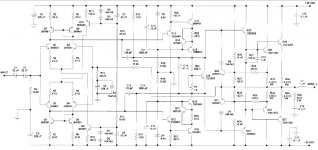
Hm... I found this in a book, but not much explanation about it is mentioned, so I would like to understand about the basic structure/topology of it.
Well.... I personally interested in its VAS. (Area which around Q11-18)Haven't seen something like that... seems cool too
Also several thing that doesn't understand/clear, such as :
(I) Function of Q20/21 (is it some kind of local FB ?)
(II) Bias spreader(& thermal tracking) is made up of Q19, R23 & P1.
(III) what is the use of C6 & D3, D1, 2, 4 & 5 ?
Attachments
To who should we credit this design? I too am just learning, so I have captured this and look forward to some knowledgeable feedback. (sorry about that)
DI etc sets the voltage for the constant current sources Q9 and Q10 tha feed the LTP's of the input. That much I understand. WIKI constant current source, long tail pair, and current mirror
I think what you need to know here is that the voltage across the base and emitter of a turned-on transistor, or forward biased diode is always 0.7V.
Q20 and Q21 are controlling the quiescent current in R32 and R33 for instance. This is the bias current on the emitter resistors of the output transistors, and controlling the Class A/B current. Increase the current in the emitter resistors and it idles hotter and more into hot Class A operation.
Q19, R23 and P1 are actually used to set/adjust this current. If R23 and P1 had the same value, the voltage across Q19 would be roughly 1.4V.
D1, 2, 4 & 5 are simple 1.4V biasing for Q9 and Q10, giving 0.7V on R10 and R11. The 1N4148 signal diodes do the work, the capacitor is added to keep it constant when the mains rail fluctuates a bit. Because diodes are not perfect, and the voltage varies a little with exact current.
C6 is a rather horrible, but typical use of an electrolytic in a feedback loop. The 1N4148 diode protects it from excessive reverse biasing and will be extremely non-linear with big feedback signal. I don't like that diode much, but it may have an element of protection from the output locking to a rail too.
Last edited:
Yet another iteration of Slone s hasardous symetric differential using
current mirrors as differentials s load.
These kind of amps works hasardously , depending on some components tolerance.
This has to be redesigned to provide reproducible behaviour.
current mirrors as differentials s load.
These kind of amps works hasardously , depending on some components tolerance.
This has to be redesigned to provide reproducible behaviour.
Q20 and Q21 are controlling the quiescent current in R32 and R33 for instance. This is the bias current on the emitter resistors of the output transistors, and controlling the Class A/B current. Increase the current in the emitter resistors and it idles hotter and more into hot Class A operation.QUOTE]
No, Q20,21 and associated devices form a single slope protection scheme.
Brian.
Uh-oh, not again. I hope you're not trying to build this. It's a well known BAD design that just plain doesn't work. It was originally published by Randy Slone in one of his books, but sadly has also been copied by other authors. That said, it's still interesting to look at how it's supposed to work and why it doesn't:Hm... I found this in a book, but not much explanation about it is mentioned, so I would like to understand about the basic structure/topology of it.
Signal path A:
D4, D5 and Q10 form a constant current source that feeds the tail of the LTP input stage comprised of Q3 and Q4. The output of this is connected to the mirror consisting of Q5 and Q6, and feeds the voltage gain stage (VGS). The VGS consists of a darlington pair (Q12 and Q18) cascoded by Q16, whose collector drives the output stage. Q17 looks like a mistake. For now, let's just pretend it's not there. (I'll get back to it later)
OK - so far so good. If that's all there was to it and the VGS was loaded with a current source at the top, it would work fine and look pretty normal. However there's also....
Signal path B:
...With D1, D2 and Q9 forming the current source, Q1 and Q2 forming the LTP, Q7 and Q8 forming the mirror, and Q11 and Q13 forming the darlington pair, which is cascoded by Q15 (and Q14 being the mistake). Again, this would work on it's own if the output from Q15 was loaded by a current source.
This amp's using both though, so it's a symmetrical design, with the top half being a mirror image of the bottom half. There's ways to get symmetrical designs right, but this isn't one of them. The problem here is that the idling currents of the VGSs is completely undefined.
In a 'normal' amp with just one of everything, if the VGS was drawing even a slightly wrong amount of current, that would cause the output voltage to move away from zero, and the global feedback would act to correct the error.
In this amp, both VGSs can be drawing way too much (or too little) current and the output can still be at zero volts. The feedback will make sure the currents are the same, but not that they're correct. Since the VGS darlingtons have a very high gain, they're very sensitive and any slight imbalance in the input stages will result in them either both being switched off, or both being switched on way too hard.
Getting back to the 'mistake' transistors:
Maybe they were supposed to be current limiters for the VGSs, or maybe they were supposed to regulate the average VGS current (to avoid the problem above), but either way they're connected incorrectly. To do either of those things, they'd have to adjust the bias of the darlingtons. As it is, all they can do is try to switch off the cascode transistors.
I) Q20 and Q21 provide protection for the output transistors. Looking at the top half: If Q24 tries to draw too much current, it will switch on Q20. Q20 will then steal base current from Q22, preventing the output stage from being switched on any harder. R25, R26, R27 and R32 determine the maximum allowed output current.(I) Function of Q20/21 (is it some kind of local FB ?)
(II) Bias spreader(& thermal tracking) is made up of Q19, R23 & P1.
(III) what is the use of C6 & D3, D1, 2, 4 & 5 ?
Note that R25 adjusts the threshold depending on the output voltage. E.g. when the output voltage is very high (positive), then Q24 (and Q26) will be allowed to carry a much higher current. This kind of protection circuitry is quite common, and normally referred to as a 'slope limiter'.
II) Yes. Note that the variable one is the between base and emitter (rather than between the base and collector). This is so that if the trimpot fails open circuit, the output stage is switched off (rather than catching fire).
III) D1,2,4,5 were explained already. For the rest, let's look at the feedback network: R15 and R12 form a potential divider that feeds about 1/30 of the output voltage back to the input, so the voltage gain of the amplifier is set to about 30.
If C6 and D3 were just replaced with a wire link, this would work OK but you might have a problem with DC offset at the output unless you were careful with parts matching etc. Adding in C6 rolls off the gain of the amplifier at very low frequencies so any DC offset at the input won't be multiplied by 30 at the output. I guess D3 is there to make sure C6 never has significant reverse voltage across it, although that shouldn't happen anyway.
P.s. John Curl is a big fan of symmetrical design for power amps. Nelson Pass's F5 is also a good example of a symmetrical amp done right. (very different design, though)
[edit]: Sorry for cross posts - tool awhile to type all this...
Last edited:
Yet another iteration of Slone s hasardous symetric differential using
current mirrors as differentials s load.
These kind of amps works hasardously , depending on some components tolerance.
This has to be redesigned to provide reproducible behaviour.
🙄 It never seems to go away does it. Yes, re-design. More specifically, the VAS bias current needs to have a reference because any current or voltage that is undefined in a circuit is bad news. You can replace the mirrors with resistors or establish some sort of common mode feedback scheme.😉
Last edited:
haha, seems the circuit is a bit too completed for me, but thanks to you guys, i understand more of it.
My initial intention is not to build this monster (I hate alot of component, the amplifier I built are simple, and most likely no compensation) I was trying to incorporate its VAS/VGS ^^ if it was good (since my amplifier weak on VAS)
However, is it a so BAD design that everybody is talking ? It claim to be high performance and extra low THD at 100+W RMS.
Is it bad because of only its :
(I) idle current condition
(II) capacitor on Global NFB circuit
(III) sensitive VGS/VAS ?
I guess its not a good idea to incorporate a darlington VAS ?
However, is it a so BAD design that everybody is talking ? It claim to be high performance and extra low THD at 100+W RMS.....
I guess its not a good idea to incorporate a darlington VAS ?
I worked on this topology more than 10 years ago, before the internet. Obviously at that time, I had no knowledge about Slone's design.
In SPICE, it works. When I prototyped it, it blew up. To get it to work, either remove the Current Mirrors or remove the Darlingtons in the VAS. I found out the hard way that in this type of "Symmetrical" circuit, to have Mirrors in the 1st diff and Darlingtons in the VAS, the current in the top and bottom half must be exactly the same. Quite impossible in a real circuit.
Thanks for sharing with us your working experience. Seems the current is too high with VAS ? Incorporate some potentio to tweak current in both side would be better ?
Not possible to tweak currents to be equal. It's one of those things that works in SPICE where ideal models are used. In the real world, components are not perfect.
about the amp.
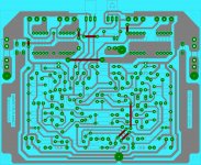
last year I made a pcb for randy sloan's class A.I have made the pcb but never got the chance to fill it with parts.the input stage and vas stage are much similar but the topology is an emitter follower design which you presented.it came from the same book if you want to try sloans amp I can give you the foil pattern but I must warn you that it is never been tested.
I have built many sloans amp and I must tell you that Im very satisfied with it and it is very stable.sloans uses parts that are common and available on most suppliers.the reason why I never got the chance is that I have built harrison symef amp.I have design the pcb and actually built it with pictures to prove that his amp is working.
there's also a picture of two optimos amp which randy sloan designed and every new years eve this amp. plays so loud until now it is working and never been repaired.
you could also try harrison symef amp. and I will tell you that you will not regret it.you could read my feedback on symef amp.
attached is the pcb for sloans class A.If you want it I could send it to you by email.
regards,
drowranger
Attachments
I worked on this topology more than 10 years ago, before the internet. Obviously at that time, I had no knowledge about Slone's design.
In SPICE, it works. When I prototyped it, it blew up. To get it to work, either remove the Current Mirrors or remove the Darlingtons in the VAS. I found out the hard way that in this type of "Symmetrical" circuit, to have Mirrors in the 1st diff and Darlingtons in the VAS, the current in the top and bottom half must be exactly the same. Quite impossible in a real circuit.
Not possible to tweak currents to be equal. It's one of those things that works in SPICE where ideal models are used. In the real world, components are not perfect.
No surprise here. In the real world, transistors have thermally dependent variables, like Hfe and Vbe. The moment a transistor begins to conduct, the temperature changes and so do these variables. A circuit that is designed around these parameters being static is doomed. I think Mr Slone published this circuit as a theoretical design for discussion and understanding not for actual functionality in the real world.

hm..... discussion.... my transistor also suffer some variable from thermal, but still consider stable >.<
sloans class A
Sloan said that all six output should be mount on main heatsink and transistors that monitors the resistor emitter should be kept away from heat.
sloans is considered as one of the best engineers of ZUS amplifier.
Sloan said that all six output should be mount on main heatsink and transistors that monitors the resistor emitter should be kept away from heat.
sloans is considered as one of the best engineers of ZUS amplifier.
Last edited:
I believe Cordell provided a solution to this type of arrangement. By placing a resistor across each of the differential pairs and including a 'helper' transistor in each LTP current mirror a defined bias current can be established in each VAS that is related to the LTP tail currents. I'd imagine a regular current mirror and no darlington VAS would likely work as well (I'd still load the LTP differentially with a resistor), or forgo the mirrors and use resistive loading of the LTP. I think for it's complexity one can do better with a simpler design. I've seen many examples here of amps that are more elegant.
- Status
- Not open for further replies.
- Home
- Amplifiers
- Solid State
- Understanding of this completed circuit ?