Except for First Watt F7 which uses only 4 actives, including a pair of Lateral Mosfets for the output stage.you can't compare with First Watt, they all use Vertical mosfets, which don't have the same unlinear input capacitance problem that Lateral mosfet have, see the ciss curves in the datasheets....
Yes please. This will make it much more accessible to a wider audience.I we pivot away from the matched LSK489/LSJ689 devices, seems like it would be worth providing provisions for LSK170/LSJ74 and J113/J176 on the PCB.
Any thoughts on this?
Lineup, sure you know this, but even in a given Idss grade, the actual Idss varies quite a bit, and you must select matches from a batch. This gets expensive unless there is a group buy. With cheaper JFETs (or source resistors) you can alleviate this problem.

Matched LSK170 and LSJ74 are available at the DIYAudioStore: https://diyaudiostore.com/collections/jfets/products/matched-jfetsI we pivot away from the matched LSK489/LSJ689 devices, seems like it would be worth providing provisions for LSK170/LSJ74 and J113/J176 on the PCB.
Any thoughts on this?
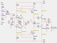
Here is the current schematic for LSK170/LSJ74 version.
The only difference are the two 100pF compensation caps.
The distortion is in fact little lower: THD 0.00029%
Attachments
LSK489 is a matched pair in one monolitic package. Have 6 legs. TO-71Yes please. This will make it much more accessible to a wider audience.
Lineup, sure you know this, but even in a given Idss grade, the actual Idss varies quite a bit, and you must select matches from a batch. This gets expensive unless there is a group buy. With cheaper JFETs (or source resistors) you can alleviate this problem.
LSJ689 ia a matched pair in one monolitic package. Have 6 pins. TO-71.
So, there is no problem. Like several think.
The current will be the same in all the 4 JFETs.
Question for the experts: The NPNs should be matched and PNPs should be matched. Is there a need or benefit with matching the Idss of the NPN and PNP?
I like that soft cliping response to , it is as in some good designed tube amp , but what interest me is the simulated THD vs Output power ratio plot , from zero Watt up to cliping point , for which I believe that is also prety flat , IMO thanks on the first place to rich biased OPS (~500mA) .I ran some sims with LSK170/LSJ74. This includes Hennady's suggestion to reroute the drains of Q1.2 & Q2.2. The feedback ratio was reduced to maintain gain and phase margin. I really like the clipping response. There's some overshoot on the square wave response, but not a lot of ringing.
Best Regads !
Yep. They're about twice the price of LSK489/LSJ689. I mentioned this earlier.
J113/J176 has the potential to be much cheaper. But I'm not aware of a source of quad matched pairs. I think it would need to be a group effort from someone interested in this project. But if done, the price would likely be much cheaper.
J113/J176 has the potential to be much cheaper. But I'm not aware of a source of quad matched pairs. I think it would need to be a group effort from someone interested in this project. But if done, the price would likely be much cheaper.
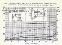
Here's some plots of 10K from 1W to 14W using J113/J176. You can see the higher order harmonics increase as it leaves Class A
Attachments


Don’t you need to match the N and P halves? In other words, you need a matched pair of LSK489 and LSJ689? If not, then it may be fine.LSK489 is a matched pair in one monolitic package. Have 6 legs. TO-71
LSJ689 ia a matched pair in one monolitic package. Have 6 pins. TO-71.
So, there is no problem. Like several think.
The current will be the same in all the 4 JFETs.
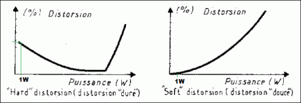
Just for general comparison , two type of THD vs Out.Power ratio plots , one is by some amplifier Soft cliping response and second is by some amplifier Hard cliping response , IMHO it is important to have very low THD around first Watt for faithfull reproduction of music microdetails ,
and here`s also THD(Dtot) vs Out.power ratio plot for one 35W ultralinear push pull OPS per se , which consist from two 6CA7 (EL 34) power tubes running in A1 class and open loop , no GNFB ,
THD consist only from second and third harmonic and less from fifth harmonic.
and here`s also THD(Dtot) vs Out.power ratio plot for one 35W ultralinear push pull OPS per se , which consist from two 6CA7 (EL 34) power tubes running in A1 class and open loop , no GNFB ,
THD consist only from second and third harmonic and less from fifth harmonic.
Attachments
Last edited:
No we do not need match the two halves.Don’t you need to match the N and P halves? In other words, you need a matched pair of LSK489 and LSJ689? If not, then it may be fine.
It is enough to match NFET+NFET. And PFET+PFET.
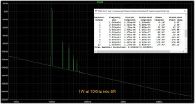
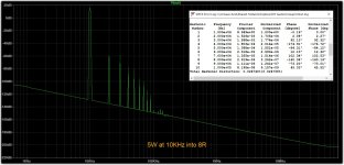
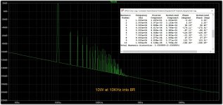
That is more than excellent results for one rich biased and simple AB class amp.Here are my numbers from testing THD at several Watt output.
I have used the LSK170/LSJ74 version i just posted.
Watt THD
01 watt 0.00029
02 watt 0.00059
04 watt 0.002
08 watt 0.005
10 watt 0.006
13 watt 0.007
16 watt 0.016
16.2 wt 0.100%
So...
LSK170/LSJ74 are available quad matched from DIYAudio store, but are the most expensive option. These have the lowest Vds range restricting users who may want to run higher rails voltages.
J113/J176 is theoretically cheaper, but a builder would need a source for matched devices. If they have to match, the economics don't look as good. Vds is a bit higher than LSK170/LSJ74.
LSK489/LSJ689 are the mid-point in price. It also has the highest Vds allowing the broadest range or possible rail voltages.
Do we think the PCB needs to accommodate all three options or can we narrow it down? The higher Vds of LSK489/LSJ689 makes me think this should be short listed to give builders more options.
We could do one PCB with LSK489/LSJ689 (SOIC and TO-71 packages) and another supporting LSK170/LSJ74 and J113/J176 pinouts
Last edited:
lineup said "...No we do not need match the two halves."
lineup, i wonder about that...
in the early days MANY years ago, jocko shared with me that the input jfet transconductances being different would make the gains of the different sides unmatched and for best linearity, it would be in my "... best interest to do something about that before closing the feedback loop." i have learned to never discount any tips from jocko and he has shared many on this site before his passing. since then, pma did some studies on the jfet quad input stage (results and background used to be posted on his web site) that helped facilitate some great discussions from john curl. and patrick has shared a nice trick to match transconductances when using n and p jfets together. of course, it depends on much work one is willing to put in to squeeze the best performance from one's circuits. many people like to say they want to make their circuits as linear as possible before applying overall loop feedback for best results, so this is another tool to help drive to that objective.
Sounds like this is a case where quad matched would be preferred for best performance, but not required? This is something that is difficult to assess in simulations, as matched NPN-PNP models are not readily available (to my knowledge).
If this is the case:
If this is the case:
- LSK489/LSJ689 is the lower cost and lower performance route (since matching the NPN to PNP is likely cost prohibitive).
- DIYAudio store quad-matched LSK170/LSJ74 is the highest cost and higher performance route.
- J113/J176 would likely be best mix of price and performance if there was a source for quad-matched devices.
- Home
- Amplifiers
- Solid State
- Ultra Amplifier with JFET input and Lateral MOSFET out